split/mixed 层 导gerber 出错
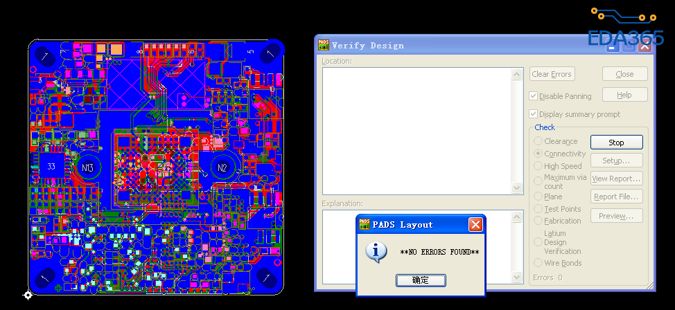
6层板,原先都是 no plane 层,做过一版。在原来基础上 top 和bottom是no plane层,中间四层改为 split/mixed 层,在lay完板后,规则检查,连接性是没有错误的,但cam中导gerber出现莫名其妙的错误,导中间四层时,会出现以下错误提醒。
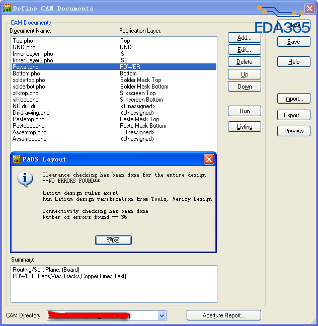
Clenrance checking has been done for the entire design
**NO ERRORS FOUND**
Latium design rules exist.
Run Latium design verification form Tools,Verify Design
Connectivity checking has been done
Number of errors found ---36
--------------------------------------------------------------------------------------------------------------------
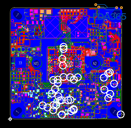
奇怪,为什么在规则检查不出现连接性错误,而导gerber时,提示连接性错误?
很不能理解,求解释,谢谢,不知道为什么传不了图片,能传的时候再传!
没有问题
可以忽略。如果觉得不爽就设置一下。
上传不了图片,可以上传文件。
确定忽略没有问题?怎么设置才不会提醒?
现在可以传了,小编,请看,谢谢
看图片猜谜?
怎么设置才不会提醒?求解,谢谢!
你同一网络分割了几个吧。
同层连接性检查。有混合平面层的PCB板,要做plane检查,为啥要把这个同层连接性检查去掉呢,去掉和不去掉有什么不同啊,亲
小编,看看老外的回答和binshenliu 是一样的处理方法。
问题:
DRC errors in CAM, but not in Verify DesignWhen I run Verify Design in PADS Layout 9.2, clearance and connectivity check out fine, but when I run CAM, I get errors. I have no way of knowing WHAT those errors are; error markers are placed on the layers, but are they clearance errors? connectivity errors? And why would there be different results in CAM than in Verify Design, don't they use the same Design Rules?
回答:If your CAM documents include Split Planes, CAM will automatically perform a Plane Check as defined in Tools > Verify Design > Plane. The settings for your Plane check may be incorrect. Go to Tools > Verify Design > Plane, click Setup. Set the selection like the screenshot shown.
总结:Okay, folks, here goes. Thanks for all the suggestions; by putting them all together in a blender, I think I've found my problem(s)
1) I have multiple planes with duplicates of some of the nets on multiple planes. So, I would end up with plane islands on one plane, but it didn't matter to me because connectivity would be made on the other plane
2) When you run the "Connectivty" check, it verifies that all signals are connected, without regard to which plane they make that connection on. BUT, when you run the Plane check, it looks for islands and flags them as an error. (This was my main problem)
3) I have two separate planes on one layer assigned the same net. They are joined together on a different layer. But, when I ran the Plane test, it saw the two separate planes as an error. The only way I can get the error to go away is by adding a "dummy" trace connecting the two planes.
Thanks to all for helping me to see the light.
Barry
---------------------------------------------------------------------------
原地址:https://communities.mentor.com/message/50167#50167