[Help] Newbie here! FM transmitter Colpitts oscillator
I am very new to radios but I have a strong interest in them. Although I have an basic understanding of how electrical components work I have
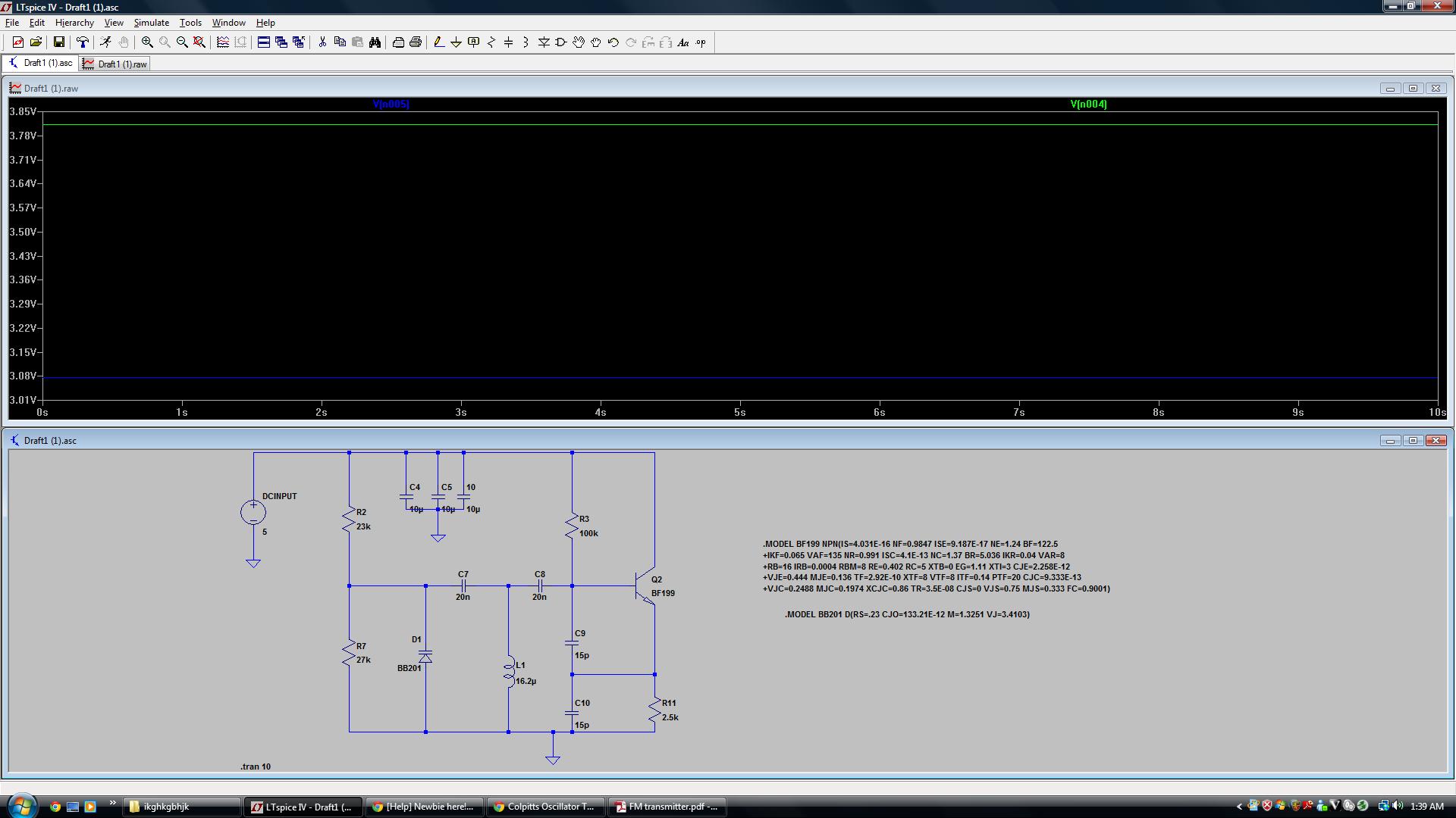
trouble putting it all together to make a working circuit. I would like to make an FM radio transmitter using a Colpitts oscilator. I found a schematic
of one such circuit online which I have added to this post as an attachment. At the moment I am just testing the Colpitts oscilator part of the circuit
on LTspice. I think it is from above R2 to where C11 is (correct me if I am wrong). I think the audio input is meant to be a square wave which I will need to
create digitally, but that is a whole other problem. for now I haven't connected any audio inputs so it is just the 5V DC voltage.
My problem is this: I am having trouble finding correct values for my tank circuit. I'm not really sure which capacitors are to be included in the frequency
equation for the Colpitts oscillator. I think it is the varactor in parallel with c9 and c10 (in series). I want my frequency to be around 46.5Mhz (so when
the signal goes through the doubler it should be 93Mhz) but when I test my run my circuit through the simulator i keep getting a constant voltage at the
output of the oscillator :(
Please help ! Thank you in advance!
The resonant circuit is C7 in series with the Varactor, both in parallel with C8 in series with C9 and C10, and resulting capacitor in parallel with L1.
C8 is a coupling capacitor and C9 and C10 are the feedback capacitors.
Oh i see now. So my capacitor value for the Colpitts frequency equation is calculated with C = (c7//varactor)+[(c8*c9*c10)/(c8+c9+c10)] ? And also, why isn't c7 a coupling
capacitor too?
Your VCO is completely wrong...
Research some books about VCOs and make you design by paying attention...
You may like to start with this. It is just an example.
Kerim
Thank you! I will study your circuit to see what is wrong with mine. But i do not know what is
.meas tran time1 when V(out)=1 cross=1
.meas tran time2 when V(out)=1 cross=3
.meas tran freq param 1e-6/(time2-time1)
used for. Also when i change the stop time and the time to start saving data in the simulation command panel, the
whole graph changes! even when i zoom in until both graph are on the same scale, the graph for stop time of 10s looks very different to the graph with stop
time 20us.
For the .meas (or .measure) command, I learnt it from the LTspice help. After you run the simulation the variable time2, time1 and freq as defined will be given (their values) on the "Spice Error Log" (listed on the 'view' menu). So you need to open it and search the lines on which these variables are written with their calculated values.
For instance, time1 is when V(out)=1 for the first time on the displayed trace (cross=1) while time2 is at the third time (to get a full cycle). Obviously we can use cross=6 for time1 then cross=8 for time2 and the difference will be the same. So I let LTspice calculate for me the frequency (as freq) which is equal the inverse of the period (time2 - time1). The factor 1e-6 is just to get MHz instead of Hz.
About the stop and end times, you are right the trace changes. The same happens when we like to view a trace on an oscilloscope by changing the time on the X-axis. If we let the start time be zero, we can see the rate of the oscillation growth till it reaches its steady state.
If you compare two traces for the same signal, one without zooming and another with zooming, the former is the good one since it has a better resolution during the calculation of its points.
Thank you!
I want to change the voltage bias for the varactor to around 2.7v so it will be in the linear region of operation and allow for some swing when I add in the square wave.
Did you just play around with the values for the capacitors until you got approximately the right frequency? Or is there a more accurate way of finding values, like what vfone told me :D?
Before I had a simulator, I used to calculate and recalculate the value of every component after every test on the real circuit till I get a reasonable response I was looking for. Now I just do some preliminary calculations then I let the simulator helps find the optimum solution though its result depends on the models used on the simulated circuit. Later some further and final adjustment will likely be needed too on the real circuit (for high frequency, the layout of the PCB will also affect the function of the circuit).
About the modulating signal, I am afraid a perfect square wave cannot be carried unless the transmitted bandwidth is much larger than of the fundamental frequency of the input signal.
what are your preliminary calculations?
Freq = 1/2/PI/SQRT(LC)
The feedback ratio C9/C10 is about 1/10 though other values work too.
I chose R3 and R11 so that collector (or emitter) current be close to the nominal value (from the datasheet). It is about 3 to 5mA. I think in this example is about 3mA.
For instance, although the circuit oscillates, this doesn't mean it is good for modulation. Its frequency selectivity should not be too high to allow the required frequency deviation without appreciable change in the output amplitude. This can be tested by adding the modulating signal, preferably sinusoidal during the first tests.
is it C = [(c7*varactor)/(c7+varactor)]+[(c8*c9*c10)/(c8+c9+c10)] ?
L1 has two equivalent capacitances on its two sides:
(Left) varactor and C7 in series
(right) C9 and C10 in series
For 2 series capacitors C1 and C2:
Ceq = C1*C2/(C1+C2)
Then the two sides are added since they are in parallel.
You can neglect C8 but if you like to insert it, you can recalculate the right side as C8 and Ceq (of C9 & C10) also in series.
On the real circuit, C9 or L1 may need to be calibrated.
What I didn't calculate is C7 so I let it be 1p
The main role of C7 is to let the varactor change the frequency with the required deviation. So when the modulating signal is added with a suitable amplitude, one may test different values for C7. The same for R2 and R7 while keeping their sum about 50K for example.
For instance:
C = [(c7*varactor)/(c7+varactor)]+[(c8*c9*c10)/(c8*c9+c9*c10+c10*c8)]
after you did your preliminary calculations did you still have to calibrate the capacitance values a bit? Because i keep getting 1.25uH for my inductance after using:
Freq = 1/2/PI/SQRT(LC) = 46.5Mhz (but when i simulate it it is 47Mhz)
C = [(c7*varactor)/(c7+varactor)]+[(c8*c9*c10)/(c8*c9+c9*c10+c10*c8)]
c7 = 1p
c8 = 100p
c9 = 10p
c10 = 100p
varactor is biased at 2.7v ~65pF
oh i got it now! thanks for your help!