ASK modulator using Opamps
Attached is the snapshot of the schematic of ASK modulator.
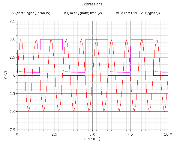
I have attached the plot too.
I am not getting where the mistake is but I hadn't get the desired output.
Please correct me and help me to get the desired ASK modulated output.
Thanks!
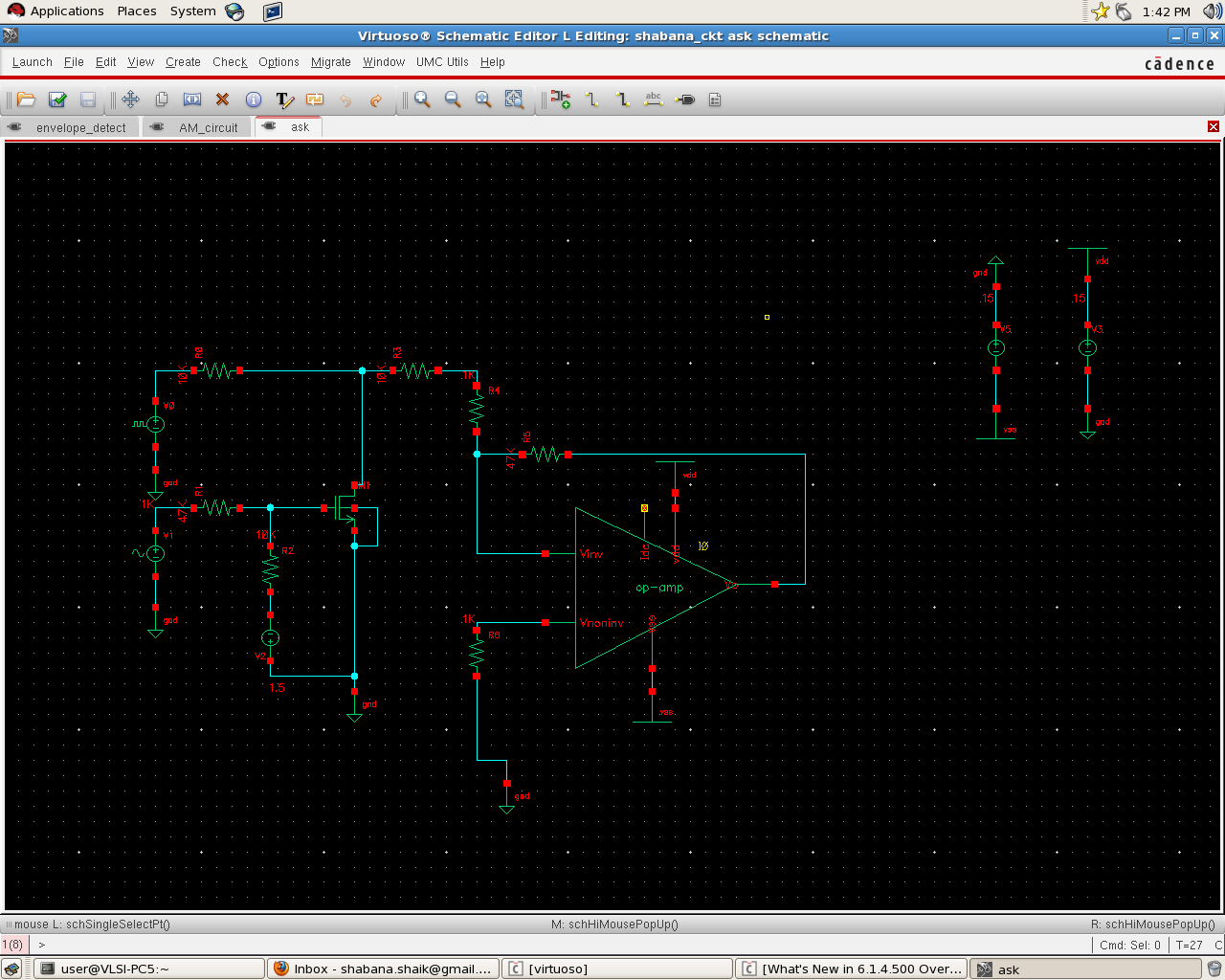
Without any net names in the schematic, we can only guess about waveform assignments. But the symbols suggest that you mixed up V0 and V1. In addition, did you consider that the M1 substrate diode will cut negative signal voltages?
Hi FvM,
V0 is carrier signal and V1 is message signal.
V1 is sinusoidal signal and V0 is pulse. Clamped square wave is the modulated output measured at opamp's output terminal w.r.t gnd.
I didn't consider the M1 substrate diode concept.
I want to send this ASK modulated signal to the tag antenna and want to check the power extracted by tag, back scattered modulation and others.
As a first step, i tried to check ASK modulated output so that once the output is correct, i can implement the same with HF range and proceed further with my analysis.
Hope u understood my point.
ASK is basically a binary modulation. I don't understand how you want to modulate a square wave carrier with a sine message. In any case, the square wave should control the switch.
In simulation, you can use behavioral components like ideal switches, controlled sources and possibly multipliers. You don't need to refer to OPs or transistors. A real reader cicruit will look quite different anyway.
Hi Fvm,
Sorry, Sine wave is the carrier and pulse is my message signal.
FVM is right, you have your circuit backwards. The drive to the FET should be your digital signal. The FET will short out the sine wave when it is ON, and will pass the sine wave when the FET is OFF.
Also, to actually send data on the sine wave carrier, the sine wave frequency has to be much higher than your data rate! Try the sine wave at 20x your data rate at least.
Actually, I have traversed the signals now compared to signals shown in image.
What are the other changes to be done to make the circuit to work? yeah, as u said, I will change the carrier frequency 20x times more than input signal.
Moreover, how to give digital signal/inputs in spectre cadence?
I thought pulsating waveform will do and work as digital input.
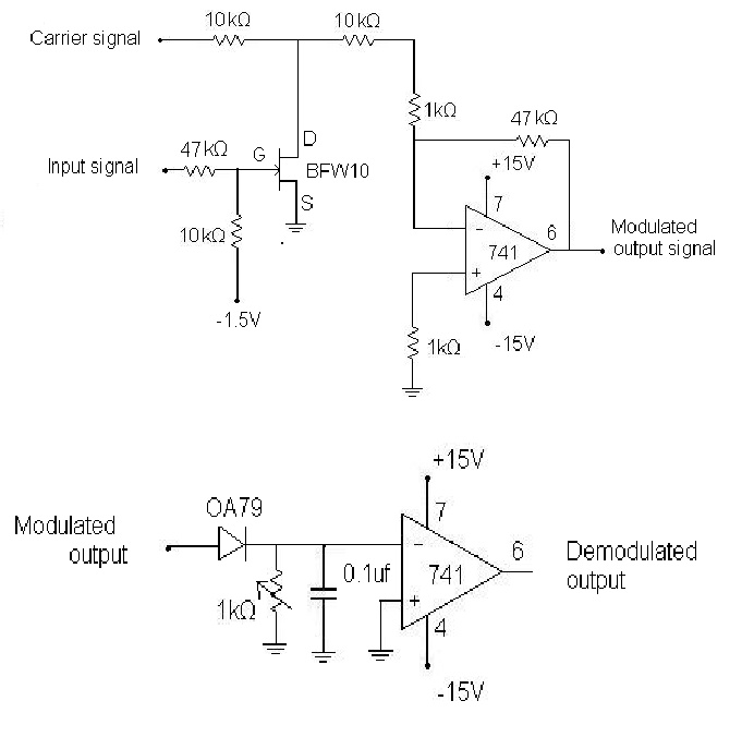
I have attached the original modulator circuit given in a paper.
Thanks!
---------- Post added at 14:05 ---------- Previous post was at 13:48 ----------