finline_ground_structure
时间:04-06
整理:3721RD
点击:
Hello,
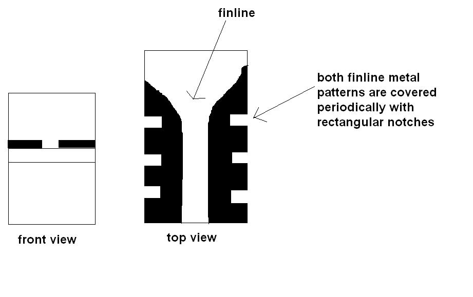
the attached picture shows a transition from finline to hollow waveguide (metallization = black).
Does anybody know the reason for these ground structures ?
-e
the attached picture shows a transition from finline to hollow waveguide (metallization = black).
Does anybody know the reason for these ground structures ?
-e
May be another picture for better illustration.
looking in 2nd picture of transition from finline.
@maurymw
the picture on the right side shows the transition from unilateral finline (bottom) to hollow waveguide (top).
The whole substrate is placed in parallel to the electric field maximum of TE10 mode in hollow waveguide.
really ? No ideas ?