Need Help about Bypass Capacitor RF Power Amplifier
时间:04-06
整理:3721RD
点击:
Hi all, I want to design a RF power amplifier using Doherty configuration. At each of the main and peak amplifier, I intend to make a bypass circuit in order to allow high-frequency go to ground (so not disturbing the power supply and output port). Here is the detail of the circuit I'm about to design :
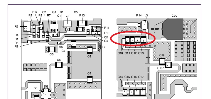
I adapt the circuit from NXP Application note.
My question is, what is the line between the the drain and the bypass capacitors (those I circled red in the picture)?
Is it a microstrip line of certain Width and Length? If the line has some purpose, how do I calculate the right W and L in order to conform with the purpose?
Thank you. I appreciate your help.
- How the output power changes by varying the capacitor connected in series with gate
- DC blocking capacitors or interdigital capacitors at 24 GHz
- Why do company sites have inductors and capacitors in an s2p file format?
- DC block connector vs capacitor
- How to choose the right capacitor?
- What type of resistors, inductors, and capacitors to use for 2 GHz LNA design?