Can I use active loop filter here ?
"initial time" sounds like referring to a pure simulation problem. A real PLL design should be able to recover from any state. Usually it's sufficient that the active filter is free from gain reversal.
ya thats f9. But in an active LF, the feed back path from -ve i/p terminal to o/p has cap. So how the opamp will get its common mode.
I can imagine many active filter topologies, you should show your circuit.
Integrators are commonly used in PLL's to stabilize the loop But the initial condition with power-on or siignal-on will depend on several factors.
In order to make the design survive you must minimize the VCO error to be within your PLL capture range, so initial condition must be considered random.
Some people use dual mixers or dual/variable gain compensation to permit wide capture range and then slow tracking for low jitter.
Sometimes a Frequency detector is used which suffer from more edge noise and jitter but requires a signal that is suitable for mixing with VCO and also locks in phase as opposed to 90 deg phase offset in the so called Type I phase mixers.
The capture range is determined by the loop characteristics. Often a series resistor is added to the cap to give proportional gain and wider capture range at the expense of jitter and then a parallel Cap at 10% of the main integrator cap value to provide lower ripple and VCO jitter.
I will catch some sleep and let you re-phrase your question but I don't believe initial condition is the real issue.
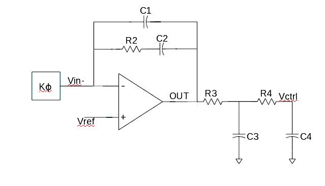
If this kind of Active filter is used.... how Vin- will get the Vref, as there is no dc path from o/p to i/p. In that case my Opamp might enter into linear region
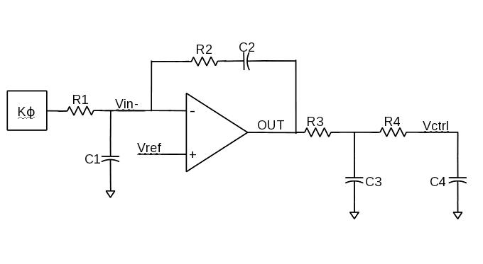
As guessed by SunnySkyguy, it's an integrator (or more exactly a filter with PI characteristic). The feedback loop over VCO and phase comparator will generate an input signal that brings the integrator output into midrange.
Conditions to be met: 1. the loop has correct gain sign, 2. the frequency programming is within the VCO range, 3. the phase comparator has a monotonous output over the VCO frequency range.
Hi... thanks for your valuable suggestions... I indeed found that the PLL loop itself take care of the biasing part. I have a model to analyze the stability, in that model I have tested the 4th order active LF with a VCVS as amplifier. After stabilizing the loop, I put my LF in Transient model and it worked fine. But how to do the stability analysis with practical amplifier ? As it wont have any kind of gain in AC simulation. Also in AC simulation any initial condition wont work.. PLZ help me
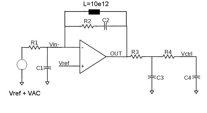
Stability analysis requires a PD & PLL model. It can be designed to include a DC feedback. To analyze the amplifier gain on it's own, you'll want an auxilary DC feedback in the analysis setup. It can be easily provided by huge inductors or other virtual circuit elements.
You can also close the loop by a series voltage source and calculate the loop gain as a voltage ratio.
Yes, this alternative resembles one part of Middlebrook's "General Feedback Theorem" (GFT) - however, this works only in case the series source is placed at a node where a low output resistance meets a high input resistance. Preferably: Opamp output.
The problem isn't exactly clear. To analyze the amplifier gain without a feedback loop, you'll just add an input source and a bias path. The bias path must not affect the AC analysis. A LC circuit would do in the present case, but controlled sources can be used in addition if you prefer.
- - - Updated - - -
P.S.: You can measure amplifier gain like this:
My concern is... I have put active LF with vcvs as amp. But when I used practical amp in place of vcvs, my PLL loop is becoming unstable. As my BW is <1MHz... I dont think my amp's parasitics can affect the LOOP stability..
Attachment 80032
If I want to put this LF in PLL, how can I do the stability analysis. As there is no dc path from i/p of amp to o/p of amp, the LF(amplifier) wont get its operating points in STB or AC analysis.
Single or double supply for the opamp?
It's still unclear what you want to achieve.
Filter transfer characteristic can be easily analyzed by the methods mentioned above.
For an analysis of complete PLL loop, you'll need a VCO + PD model. In this case, the model will provide the feedback from filter output to filter input and also the DC operation point.
Can you describe your observations precisely?
If you perform an ac analysis under closed-loop conditions no problems with the dc operating point are expected. However, you must take care that the dc loop remains closed. For this purpose, several (classic) methods exist.
First I run the Transient analysis and stability too with VCVS as amplifier in LF. I got good results. But whenever I replace the VCVS with a folded cascode amplifier, the results are not expected in Transient. Then I thought of doing stability analysis with that practical amp LF. But I think due not getting proper biasing, the loop is behaving abnormally. So, the conclusion is whenever I am using VCVS as amp, everything working fine, but as soon as I am using practical amp, the loop is not giving proper result
- - - Updated - - -
vdd and vss (1.2V and 0V)
- - - Updated - - -
As you can see the PLL have 2 loops. 1 is of PLL itself and the other is from -ve feedback loop of LF amplifier. By putting an inductor I can close the amp feedback loop. But in that case, I am getting abnormal results.
Did you check the amplifier parameters first? E.g. suffcient common mode range, no gain reversal?
Ya, its done
As in PLL with all practical components we cant run ac analysis, we need to model it. If I use practical amp in active LF, we also need to model amp. As I have seen its impossible to give proper dc voltage to amp. So how to model amp for PLL