Question about DB6NT's frequency doubler. What is purpose of wide areas? (have photo)
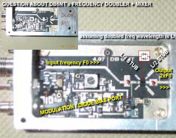
Frequency F0 going from left to right until doubled. From left to right:
1. "?" widened microstrip area
2. modulation DC bias
3. L/4 stub for filtering 2xF0 frequency out (L is wavelength of 2xF0)
4. antiparallel diode pair for mixing/doubling purpose
5. L/2 stub for filtering F0 (acts as L/4 stub for F0)
6. again some "?" widened microstrip area.
So what the purpose of two widened microstrip areas? I guess it is not quarterwave matching line.
It looks that it is quarter-wavelength (for 2F0 before diodes and for F0 after diodes).
If it is some kind of unwanted freq reflection method, what impedance of this lines i must choose?
Thanks!
Such wider sections are low-impedance matching sections.
Is it for reflection purposes?
I tried some calculations and here is my guess:
1) assume that most of microstrip is 50 Ohm, and Er of substrate is about 2.65
2) left widened section: Quarter-Wave length (for 2F0), about 5..6mm wide. Z1=15 Ohm. It is special mismatch section to reflect 2F0 back to right area
3) right widened section: Quarter-Wave length (for F0), about 3..4mm wide. Z1=22 Ohm. Again special mismatch to reflect F0 back to left area.
So leakage of F0 to doubled area is minimised (and leakage of 2F0 to F0).
Am i right?
I think you are right. An experiment can show if you really are. You can use movable stripline sections made of a thin copper sheet to optimize the mixer, then make a final print for sale like DB6NT did