Problem with bounding area layer in ADS2011
时间:04-05
整理:3721RD
点击:
Hi!
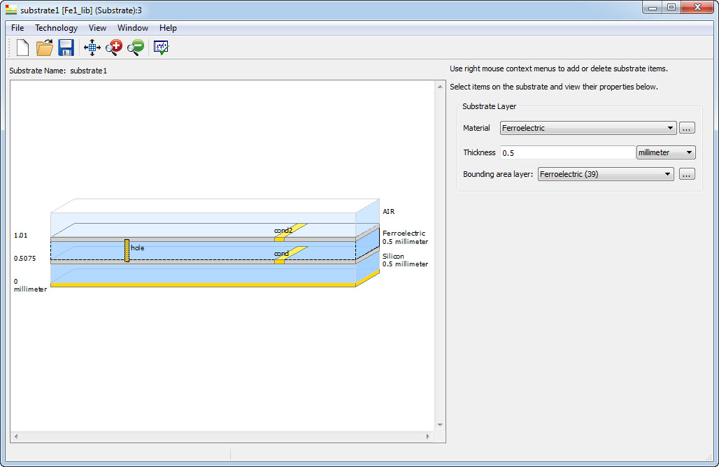
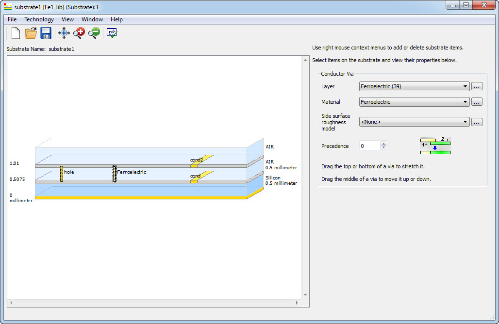
I designed a simple delay line with dielectric strips in upper layer.
I have next problem. Bounding layer not limit dielectric area. Dielectric is everywhere.
I partially solved this problem by transfer polygons in "dielectric via layer". But this structure can't be solved with help of momentum, only with FEM.
I designed a simple delay line with dielectric strips in upper layer.

I have next problem. Bounding layer not limit dielectric area. Dielectric is everywhere.
I partially solved this problem by transfer polygons in "dielectric via layer". But this structure can't be solved with help of momentum, only with FEM.
Maybe try ADS2012?
well, u built a huge 500 MHz resonator there bud. Try adding around 400 via holes from top to bottom ground layers.
Use Momentum Box.It will cover your whole structure by a closed Perfect Conductor.
For more information, read relevant help topics.