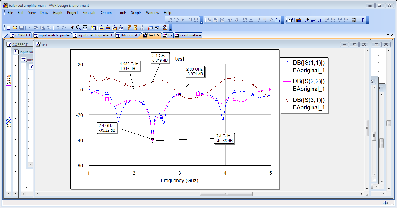
balanced amplifier result
techniques, but i think that matching network has no effect on the amplifier design since the branch line coupler had cancels all reflections.
The problem now is that at some frequency, the gain goes below 0dB, but its perfect at the design frequency. Could the problem be as a result of poor
match from the matching network used. From the graph, the input and output return loss is good. Please i need advice on the result. I am not sure if the design is good
enough.
Also, i need advice on the best method that can be used to bias this transistor(NE76038), i am thing of using radar stub or RF choke. Please help.
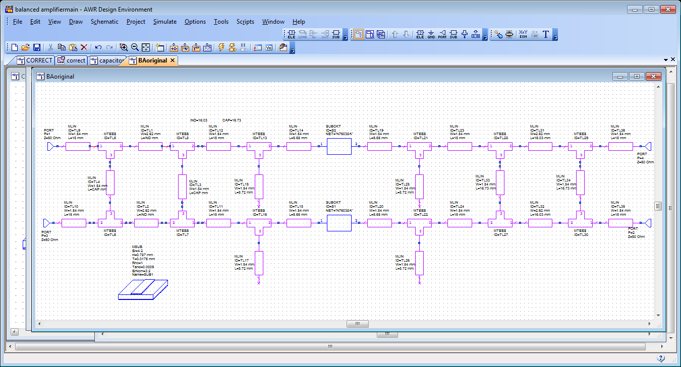
If you post your circuit diagram or better project file, we can say something..
here is the schematic
I think Your amplifier needs an optimization in the band which your are interested in.Assign widths and lengths of TLs ( of course symmetrical of each branch) being as variables and do an optimization.
You'll probably get a good result.
Thanks so much BigBoss, it is working perfectly after optimization. The gain is increased to 10dB from 2 to 3GHz band. The problem now is
how to bias the two transistor used in the design and choosing the best bias techniques.
Not true. All that a balanced amp design with rat race rings means is if the two amplifiers input and output impedances and gains are identical then any reflected power will add at passive resistor terminated port and cancel at input/output port yielding good input Z and output Z. If the amps are not matched then the whole idea is invalid.
The ampliers must have their respective impedance matching to get desired performance (gain/noise figure/IM). If the amps are identical then the gain will be 3 db greater in the balanced configuration then single amp on its own.
This is another question and design consideration.There isn't such "the best technique" instead there are some proven and proper techniques,If you search a bit you'll find very useful information about them.
The biasing circuit will supply wanted voltages/currents for the transistor almost independent from temperature effects.There are many good design samples on the internet, you may find a biasing circuit for FET transistors.
Thanks so much RCinFLA, In this design, the amplifiers are identical but inorder to get a good input and output return loss, the balanced amplifier is design for less gain than that of single amplifier . since a single amplifier has bad input and output return loss the balanced design does the magic of that, according to Pozar.
Thanks BigBoss, i finally found some really cool biased circuit, i think i am going to use voltage divider bias circuit.
- SBL-1 double balanced mixer
- Question about single balanced mixer design
- its not working with me (balanced amplifier, power splitter)
- Single balanced mixer ssb generation?
- Biasing of balanced FET amplifier. Does Rdrain_balanced = Rdrain_single / 2 ?
- Using rat-race coupler to combine balanced output of transceivers like NRF24L01,etc.