Microstrip design for 7.9GHz synthesizer
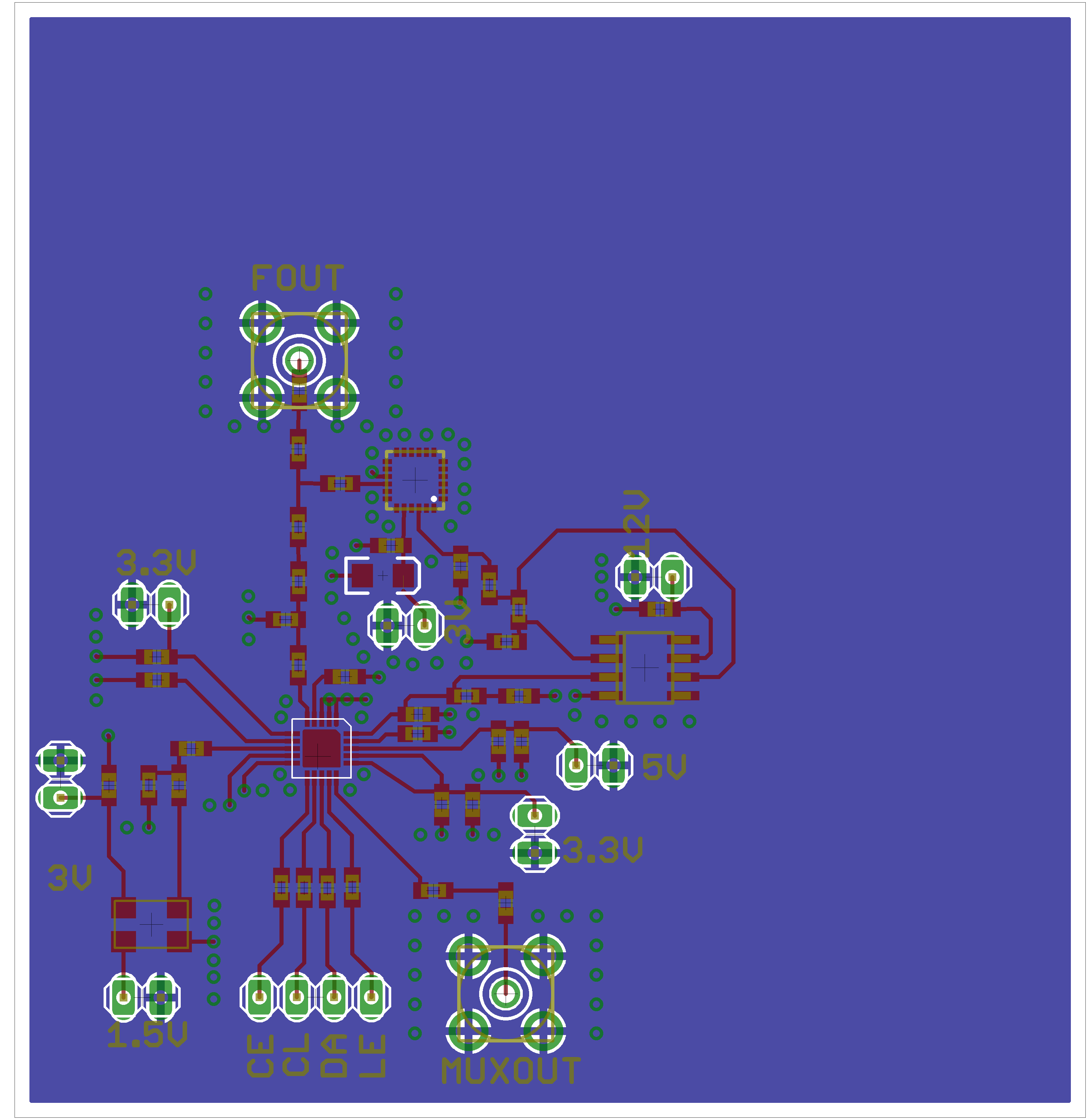
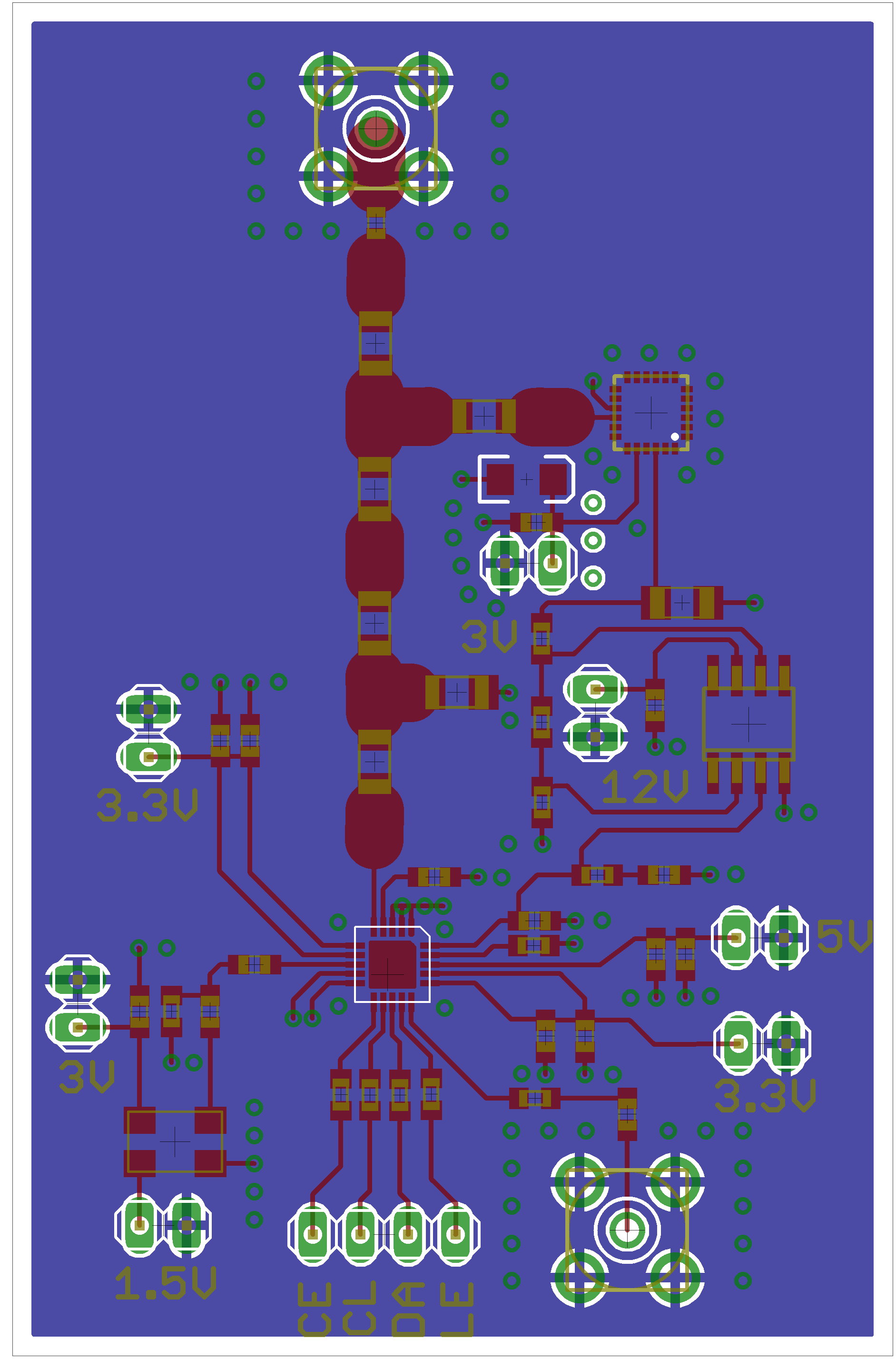
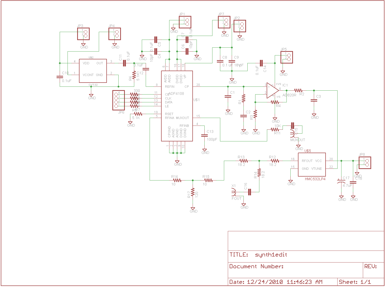
I attached 2 board layouts along with the schematic. One board layout applied the trace width and length calculated from txline while the other board layout has the connections for the 7.9GHz signal path made as short as possible.
This is my first high-frequency board that why I hope to get some feedback to improve my design. Merry Christmas and Thanks in advance.


I don't see capacitor between RFINA and R16. Replace R15 and R13 on 27 Ohm resistor. Make distances between components pads in RF paths 0,25 mm or smaller if possible. Capacitors at AVDD, DVDD, VP, RFINB must be placed as close as possible to pins. Decrease C13, C4, C6, C9 to 3 pF. Distance between line and GND pads of X1 seems very small. 2nd topology more proper but may be better. 1,6 mm is very thick, try 0,25 mm and recalculate line width.
Thanks for the reply Dr.Drew. It's just that the 1.6mm thick FR4 is the only material available at the moment. I'll add a capacitor between RFINA and R16 and I'll also adjust the capacitors later.
I am curious why R15 and R13 must be changed to 27 Ohms. It's just that the VCO has high output power of 14 dBm so my thinking is to implement a 6dB resistive splitter for the output of the VCO and then for the signal to be fed back, another attenuator stage of at least 3 dB to make the output signal power at RFINA be within the limit of ADF4108 which is 5 dBm.
Lastly regarding the 2nd topology (the one with the shorter connections) being the better one, I would just like to ask why the first board is the inferior one given that the track widths at its RF path equal to the width given by txline.
My apologies for numerous followup questions. I'm thankful I can get feedback from experienced RF designers. Looking forward to the advice of others as well. Thanks again and Happy Holidays.
It's unessentional to replace resistors but one component is more cheaply than two.
Perhaps line widths were calculated incorrectly in txline. 50 Ohm line at 0,5 mm FR4 has 0,8 mm width. At 1,6 mm it will have 2,5 mm.
And one more advice. Use AD797, AD829 or AD4898-1 and inverting connection of OpAmp. Phase noise will be smaller.
FR4 is a very poor choice for 7 GHz! To have a prayer of working, I would make the microwave traces as short as possible. I would eliminate R15, R16, and R17, for instance, as they do very little. You can make R13 a larger value to act like an attenuator. I would lay it out to put the VCO output very close the the PLL chip input. Keep the RF output connector close to the VCO also. Everything elese is very low frequency and the lengths of the traces no longer matter there.
As far as the line widths, they are all very short, so the actual width does not matter all that much. If there is a big length between R13 and the PLL input, make that one 50 ohm width. The other traces, The layout on the left looks too narrow in width, the layout on the right looks too wide a width (since all those component pads add capacitance to ground, and you will end up with lines who's overall impedance is lower than 50 ohms). By eyeball, I would use a width somewhere between the two!
Rich
Thanks for the replies Dr. Drew and Biff44. I understand that 1.6mm FR4 is not the ideal material at my target frequency range but it's the only material available at the moment. Though with FR4 being my material, I guess the short traces is my only option.
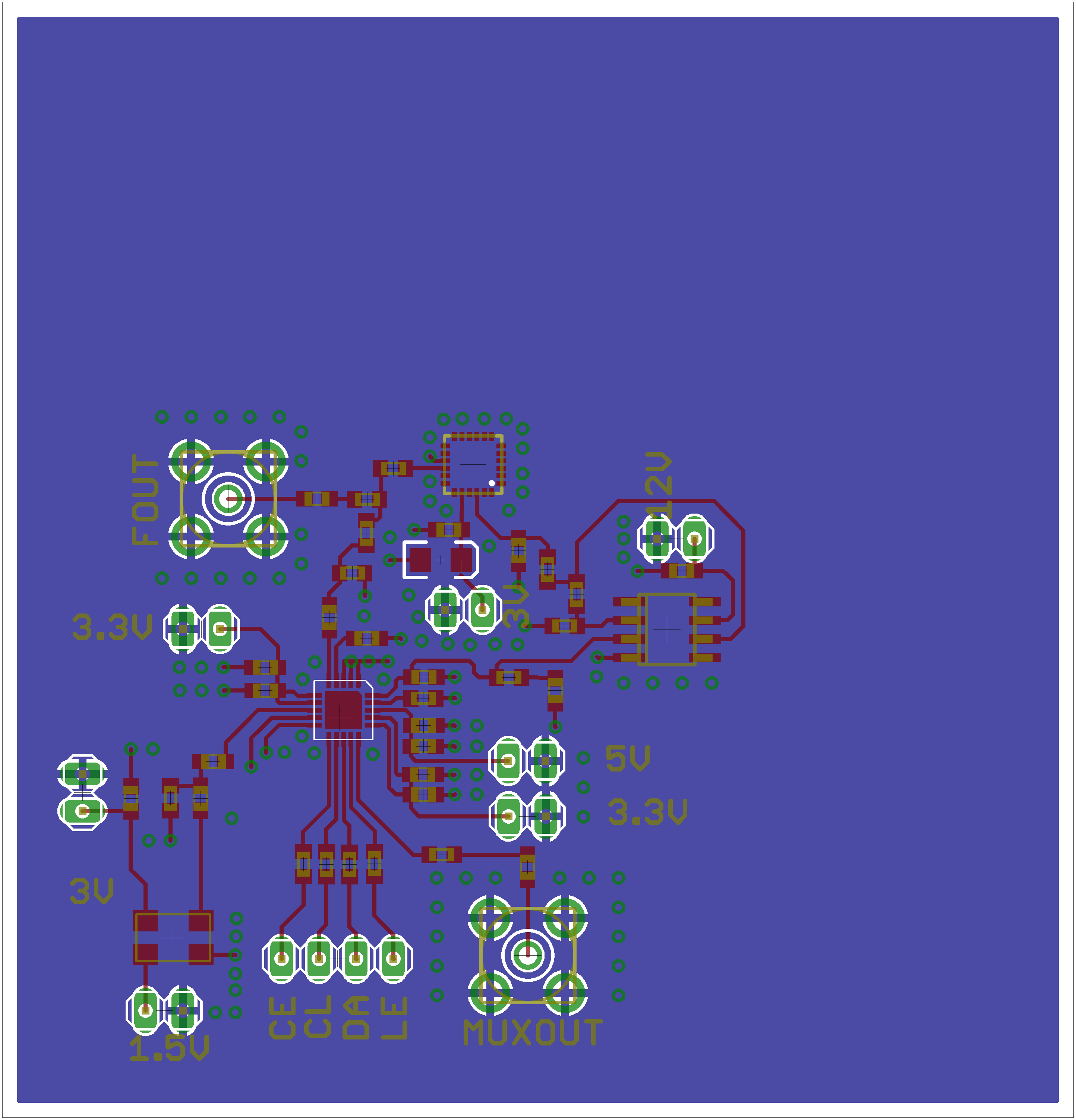
Regarding the RF feedback path, I decided to replace the original splitter and attenuator configuration with just a resistive unequal power divider. I also tried to make the traces as short as possible for the high frequency path as well as the traces to the capacitors of the supply pins.
With regards to the line widths, my intended approach was to make use of microstrip transmission lines. However, the small width of the VCO pins (among others) would not fit the 3.1mm width of the microstrip I calculated from txline. That's why I decided to adjusted the trace width to fit the dimension of the VCO pins and then roll with it in making the other connections. Should my approach be match the trace width to the VCO and other ICs when connecting to it and then make the trace width as wide as possible when connecting other components?
Thanks again for your replies. You've made Christmas much better for me. Looking forward to the next feedback I will get.
Here is the updated board layout:

1. For VCO supply, put a 100uF Tan Capacitor maybe better.
2. For CLK/DATA... etc, put a 100pF capacitor maybe better, this capacitor couldn't be higher than 100pF. You can try smaller value if can't lock, but have one capacitor is better than none.
3. If possible, use LDO for VCO/PLL/OpAmp respectively.
4. Avdd and Dvdd can be connected with inductance, say 1uH.
Good luck.
Capacitor is a poor variant for EMI supression. It will be better to use NFA or NFL Murata EMI filters.
VCO phase noise degrades because of LDO noise. Some LDO are noisy. Good variants are LT3029, ADP150, ADP151.
I used to use ADP1711 for PLL IC LDO. You should carefully select LDO.
Thanks for all your replies. You all have been a big help.
I am using low dropout voltage regulators on another board that will be connected to the board via the numerous 2 pin headers.
About the schematic, the component values are based on the evaluation board schematic provided by Analog Devices.
For the sake of discussion, I would just like to ask why the microstrip track width from txline that I implemented would not work considering the traces are all on the top layer and the bottom layer is the ground plane. Is the reason biff44 mentioned (larger overall impedance) the only reason for it not to work or are there other reasons for it?
Also from my understanding, the reason to keep traces as short as possible for the RF signal path is mainly to minimize coupling to the power supply lines. Am I correct?
Having said that, since in the latest layout there is an unavoidable long track to Fout, should I just make the track width there equal to the 50 Ohm width computed by txline?
Thanks again for all your replies. My apologies for the multiple follow-up questions.
The RF trace is like an antenna, longer trace, more radiation RF signal. Not only coupled to power supply.
Yes, you should use 50- ohm trace, but for FR4, it's difficult to do that, because FR4 Er is between 4~4.6, so you can't do it precisely. You can use taper line connect pin and 50 ohm trace.
It is necessary to make 50 Ohm trace in synthesizers preciselly? 10% accuracy is suitable.
can anyone tell me in which software ginebra has drawn that schematic diagram and layout design?
im very new to RF design, so im very pleased to any answer.
advance thanks
I used to use Altium to draw the SCH and PCB layout.
And use Microwave office to design the filter, and then import the filter layout into Altium from Microwave Office.
does Altium include ADF4108 in the library?.......i got a .bxl file from ANALOG DEVICES and converted it to Altium using ULTRA LIBRARIAN READER.
I think it's simple to draw the SCH and footprint in Altium for any component, you don't need to import from the other source.
Hello everybody,
I am trying to design 2.45GHz patch on ADS using FR4 substarte.But i am unable to find the substarate paramters i.e thinkness,height and dielctric constant.
I dnt know how should i proceed.
Could you help me design a 4900MHz Frequency synthesizer circuit using ADF4108.
It's so hard to design because manufacturer doesn't support sample schematic of this IC.
Thanks a lots !
design Microstrip synthesizer 相关文章:
