50OHM Striple line question
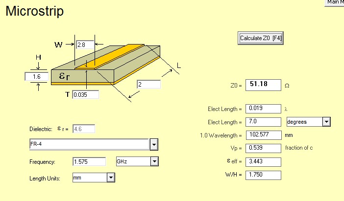
It is double layer PCB with FR4. Thickness of PCB is 1.6MM. 1oz
The result is 2.9mm width on pcb as attached pic.

However the pin spcae of this chip is only 1.2MM. how to run this 2.9MM line to antenna pin? 2.9MM is much wider than 1.2mm.
PCB as below. the green arrow point to the line at width 1.2mm only. how can it be 2.9mm for 50Ohm impedance?

I would guess you would run a 1.2mm trace from the pin, calculate its impedance, and then match it to your 50ohm 2.9mm strip.
The question now is, what impedance does your chip want at this pin ?
It is GPS signal. it should be 50 Ohm.
PCB as below. the green arrow point to the line at width 1.2mm only. how can it be 2.9mm for 50Ohm impedance?

You see in your screenshot that the effective wavelength was calculated as 102mm.
Transmission line effects are only seen when a line starts to be electrically large. For very short lines, the transmission line effects are very small. Rule of thumb: Line impedance of lines shorter than 1/20 wavelength is not critical at all. So don't worry, no need to have a matched line for this short segment.
A > 50 ohms planar strip segment can be calculated as series inductance. It can be compensated if exact impedance matching is required.
Reviewing your PCB detail, it doesn't look like you're trying to achieve 50 ohm impedance for the continuation of the transmission line. In so far, the problem doesn't seem to be particularly related to the pad geometry of the GPS module.
Usually multi-layer and/or thinner PCB substrates will allow to match 50 ohm microstrip impedance from the pad. And even for 1.6 mm double layer, the transmission line can be designed as coplanar strip with ground.
thanks so much for all above
- Limiter diode should be ground or 50 ohm?
- Matching 75ohm antenna to 300ohm receiver
- Power considerations for 50 Ohm resistors in power combiners
- HFSS - 50 Ohm Coaxial line terminated with 50 Ohm impedance boundary. |S11| too large
- 50/30 ohm coax adapter
- are 50 ohm transmission lines required for 2.4GHz amplifier?
