Falling Edge Negative Overshoot on Transmission Line
My two ideas of what is happening are as follow. 1) The negative overshoot is caused by reflections at the load, just the same as positive overshoot. or 2) the negative overshoot is caused by reflections at the source, since current flow is opposite of a rising edge. I think the answer is 1, and details of what I think is happening are below. Can anyone please confirm my thinking is correct? Thank you!
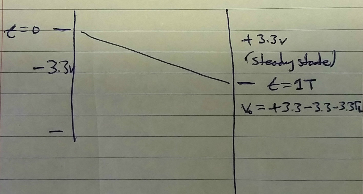
Vpp of my clock is 3.3V. Is my source essentially -3.3V at t= 0? Prior to t=1T, the load is in a steady state of approx. 3.3V.
Between t=0 and t=1T, the -3.3V wave propagates towards the load. Once at the load, the output voltage is 3.3V (steady state) + (V1+) + (V1-) ~= 3.3 - 3.3 - (3.3*reflection coeff). This is where the negative overshoot comes from (V1-).
you have given us WAY too little imformation to comment. What are you driving with, what is the load, how long is the transmission line, how are you making the measurement, what probes are you using, what is the rise/fall time.......
With drivers, usually logic 0 is lower impedance than logic 1. (except ARM they use fairly symmetrical 25 Ohm drivers from N and P CMOS gates.
When there is over/undershoot, this is usually a sign of inductive probe ground clip or signal path.
When undershoot is big with ringing,usually the driver impedance is lower than the transmission line but with high load impedance.. Applying a 200 Ohm termination should eliminate most of this to satisfy your understanding.
But if it is CMOS there will be Schottky clamp diodes. If it appears to exceed -0.5V then it is purely measurement error with probe ground length being too too and inductive.
Solution. remove probe sleeve and ground clip and use coaxial spring around barrel with outer last turn straighten as a ground probe on a ground test pin beside center probe signal pin ( solder short ground test pin on board if not handy. ) or buy a coil ground probe spring from TEK , or buy TEK differential FET buffered probes. (S)
Ensure decoupling caps are nearby on board. Breadboards are very noisy, since no ground planes and long wires.
All fast edges <0.1uS should be measured this way for textbook waveforms.