PIN-diode controlled variable attenuator


hi
see the link bellow.this is handbook of pin diode.hopefully It can help you
www.qsl.net/n9zia/pdf/pin_diode_handbook.pdf
It is not clear what topology you are planning on using, so draw a schematic of the full thing for us. If you are planning on using pin diodes as in that paper you referenced, you need a S1P file.
As you need a driver, you will need a simple variable current source to push through your PIN diode a DC current, from zero to a maximum specified current value.
Usually any variable voltage regulator can be used, with a series resistor set to limit the current at a maximum voltage it can reach.
The VVA response is not linear, it typically rises fast from zero mA , then slower to a maximum at e.g. 50 mA.
The maximum DC current usually depends on a maximum RF power your device should control; it is specified for a particular PIN diode.
Drivers recommended by VVA makers typically use opamps with a diode in feedback, in an attempt to linearize the response. You can play with many such circuits, or, you can design a DAC to get the current by a code to get a linear loss response.
Hi,
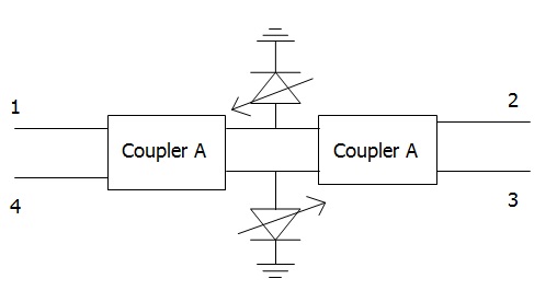
thanks a lot for the handbook.a This is the schematic that I have planed for this circuit.

Hard to get S1P for a PIN diode. Usually the simulators use the Spice models for PIN diodes.
NXP have S-parameters for some PIN diodes, but they are not presented in a table format.
http://www.nxp.com/documents/data_sheet/BAP55LX.pdf
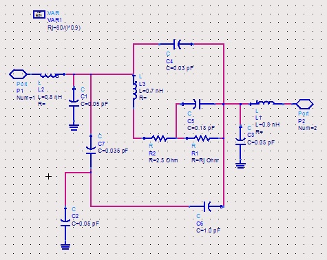
The choke is definitely necessary for the bias circuit. The topology of the bias is important for getting the best performances over wide frequency range.
http://www.skyworksinc.com/uploads/d...ts/200312C.pdf
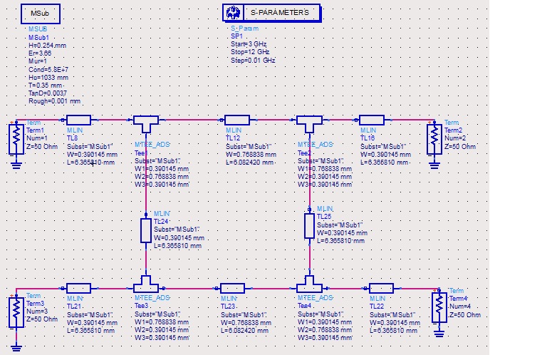
Thanks vfone for your valuable comments. I made a RF choke for 7.5GHz and implemented it in the circuit. but I think I got nothing in the output port but strangely I am getting attenuation in the port which should be isolated (4). can I get any suggestion from you now?
schematic :
output:
For 6-9GHz, you should connect all components with micsrostrip lines, and tune the lengths of the lines, to get your results.
Thanks vfone for your valuable comments. I made a RF choke for 7.5GHz and implemented it in the circuit. but I think I got nothing in the output port but strangely I am getting attenuation in the port which should be isolated (4). can I get any suggestion from you now?
schematic :
output:
If I were you, I'd design a PI or TEE circuit between two couplers.Because you change the characteristic impedance between these two couplers by connecting a single PIN diode and as a result your attenuation becomes nonlinear or irregular.Instead, using a PI or TEE attenuator between two couplers by maintaning the actual charateristic impedance will much better.
You can consider the attenuator circuits as TEE or PI resistive attenuator circuits with fixed input and output impedance.
Perhaps better choice is using different topology for the PIN network, but you can make it work even this one if you add DC blocking capacitors on each port.
Also place a resistor in series with each λ/4 transmission line (~500 ohms).
Hello, I am simulating PIN diodes in ADS could you help me with the DC biasing circuit topology? Thank you.
