Simulation of semi conductor shapes with ADS
Semiconductive and/or dielectric shapes have
been detected.
Momentum supports semiconductive and dielectric
substrate layers, but not individual
semiconductive or dielectric shapes.
In the simulation, their material will be
replaced by the underlying substrate layer
material."
ANd in meshing my shape is ignored it s like I didn't add it. if ADScan't simulate semicondutors why it gives the possibility to map a semiconductor in the substrate definition?
many thanks
Semiconductors can be defined as well as Insulators.Insert a insulator/substrate where you would and then change the dielectric coefficient of this material.
Hi BigBoss,
i didn't understand your answer very well, what's an insulator? for my simulation I mapped a smiconductor layer in the part of the definition of the substrate (attached picture)
and I drew a shape and I got the warning message that I cited.
I don't know if that what you mean in your answer
There are two different EM simulators in ADS: Momentum for planar models (2.5D) and FEM for arbitrary 3D problems.
Momentum can only handle infinite dielectrics. The finite dielectrics ("dielectric via" and "semiconductor via") are only support by the FEM solver.
To use the FEM solver option, a separate license is required. Technically, this is the same FEM solver that is also available in Agilent's EMPro product. In EMPro, the solver is driven from a 3D solid modelling editor. In ADS, it is driven from the ADS layout, with special 3D options in the substrate definition. That's why some of the substrate definitions work only for FEM, and not for Momentum.
What exactly you wanna do ? Momentum recognizes only di-electric materials and metallic shapes.If you would insert some semi-conductors or polysilicon like components, it won't work.
I couldn't understand what absolutely you wanna do with these materials..
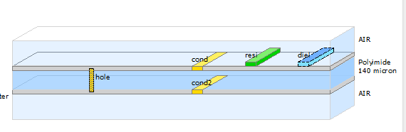
He might want to simulate the non-planar details of the BEOL.
http://muehlhaus.com/support/ads-app...3d-passivation
However, as I wrote above, this requires the ADS FEM solver (ADS option, license required) and can't be done with the Momentum solver.
Thanks for your answer
I m sorry if I wasn't clear in my question
It wasn't for a specific application, I wanted just to know if ADS can simulate shapes with semiconductor or dielectric because I noticed that we can map layers with these materials in the substrate definition.
semi Simulation conductor 相关文章:
- Semi-rigid vs flexible cable for antenna feed
- Antenna test using Semiconductor Device Analyzer B1500A Agilent
- small semi-rigid coax with air dielectric
- How to calibrate an open end of semi-rigid coax to be used as a test probe?
- need HElp: semi passive microstrip antenna for Rfid at 8GHz
- Half-mode SIW Simulation