Layout of CSRR in ADS
I want to simulation CSRR in ADS but I cann't attach rectangular to circle such as image.
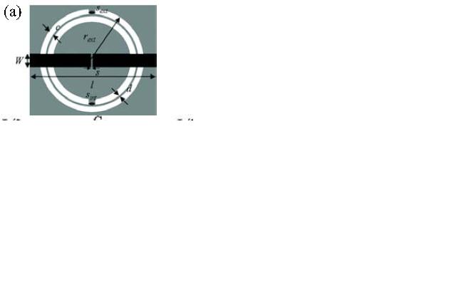
Use "Construction Lines" to draw such shapes.
Or draw in Autocad ( or any kind of CAD design tool ) and transfer it onto ADS as DXF format..
I draw circle in ADS and rectangular separately. Now, I want to attach 2shape together.
PLZzzz help me
Are these objects, the circle and the rectangle, drawn on the same layer? Do you want to add or subtract the shapes?
If they are not then they will never be able to be 'joined' together.
If you are adding the shapes together and they are on the same layer then simply select both in the layout view and do Edit > Merge > Union. This will create a new polygon that is the result of both shapes being merged into a single shape.
If you are subtracting the circle from the rectangle and they are on the same layer then simply select both in the layout view and do Edit > Merge > Union Minus Intersection. Again this will create a new polygon that is the result of both shapes being merged into a single shape that included all that is included in the largest shape with any overlap removed.
It is not possible to group the two together without merging them.
thanks for replying
I think it's not merge. circle is added or joined to rectangular
I want to draw circle in backside view and rectangular in a top of view in the same substrate
Can u help me?
Hi laperla ,
To draw on different layer, just select the different layer and start drawing. Or select a shape and select a different layer for it. Of course, you need to set up your substrate with the correct layers before doing this.
]
Thanks for replying
I want to draw in the same layer. I want to draw circle in back side and rectangular in other side of substrate
Your statement is self-contradictory. Each ADS layer corresponds to a different substrate layer.
You may need to explain in more detail if there's something we aren't understanding.
I want to simulate this paper
The advice given in this thread should be all you need.
Good Luck
I can't understand what I do. you said that I use 2layer for simulating?
Hi laperla,
As far as I can tell, this paper shows a standard microstrip topology, with a gap in the strip and a CSRR etched into the ground plane for each unit-cell. Clearly, this a two layer topology that can be easily duplicated in ADS Momentum.
You want something like this? (not to scale)
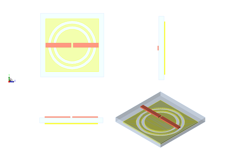
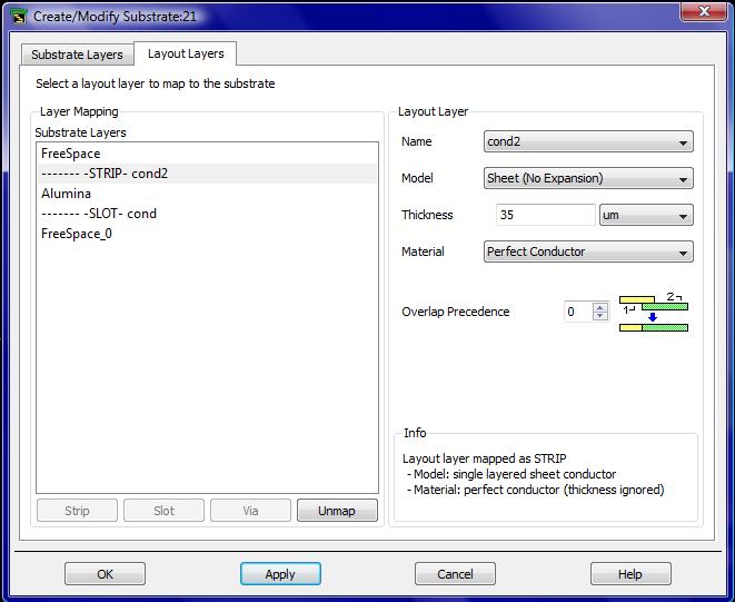
As has been posted previously even though they are part of the same substrate each pattern on the top and bottom of the substrate is draw on a different layer in ADS, for example cond on the top and cond2 on the bottom, and then mapped using the substrate definition to the required side of the substrate.
Maybe this is a more realistic view. Again not to scale.
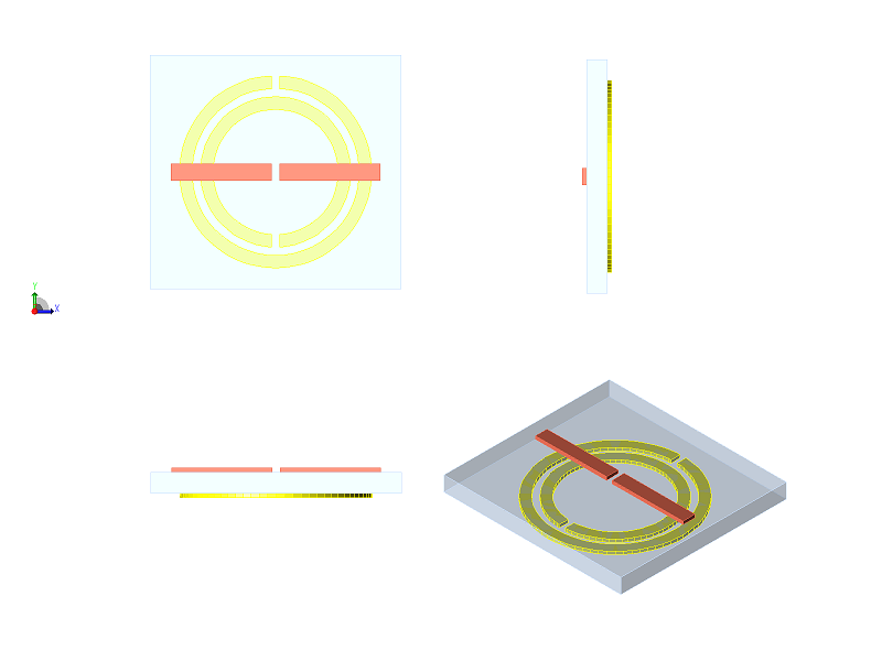
Same construction applies but opposite view of rings.
If you need to connect through the substrate to 'join' top and bottom conductors together then you need to use vias. Draw the necessary hole outline on a third layer and map that to a cunductor via through the board in the substrate definition.
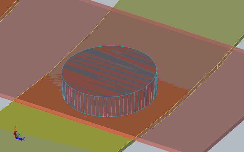
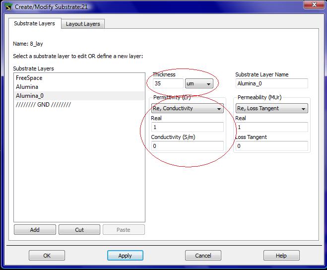
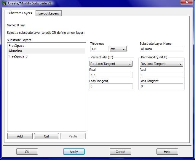
In the paper, says just one thickness for substrate but by defining cond and cond2 I have to set thickness and Er for second substrate?
Hi laperla,
In the image you've shown, it clearly says "substrate layers". You only want one layer. There will also not be a GND layer.
Hi PlanarMetamaterials
Yes, I define 2layers. how can I define layer such as RealAEL?
I want to have cond and cond2?
Hi laperla,
You might want to look up some tutorials on how to use ADS.
Remove the alumina_0 layer and the GND layer, making the bottom layer free space as well. Then in "Layout Layers" assign cond and cond2 to be the two metallization layers on either side of the dielectric.
thanks for replying
but my simulation isn't correct answer
I show set up the substrate. is it correct?
