Low noise amplifier stability, noise figure and gain
Got some screenshots attached for a low noise amplifier using an ATF-34143 FET from avago. The objective is to create this amplifer on a PCB with the following specs:
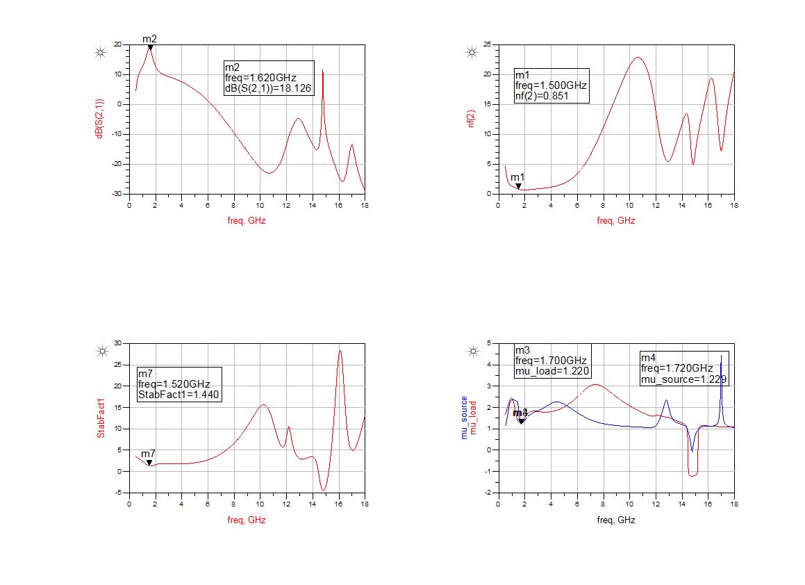
1. Unconditional stability across 0-18 GHz
2. S21 > 15dB between 1.5-1.6 GHz
3. noise figure < 1dB between 1.5-1.6 GHz
The circuit performance pic shows the K factor (StabFact1) and mu factors for stability. Everything seems fine until about 10 GHz when everything goes wild.
I'm mostly concerned about the stability dip at 15 GHz. Need to rectify this without damaging the noise or gain by too much. I've tried adjusting the component values and microstrip lengths by can't find the root of the problem. It's probably to do with the R L C feedback loop, which is needed for low frequency stability. I don't know much about oscillation but could that be the cause?
also included is a preliminary layout because the microstrip lines and vias are also factors in the stability. TL1 and TL13 are 50 Ohm lines with widths 1.5 mm and lengths 5 mm to give a sense of the scale.
Any and all help is appreciated! Any tips or improvements also very welcome
thanks


Attachment 110839Attachment 110840Attachment 110841
Why one source is grounded while the other one is not ?
There are 2 feedback loops and the problem arises from them.
One is TL4 and TL5 branch which seems ok at least but other one is weird.You put 2 inductors on Gate and Drain paths and you used 2 1pF caps. to decouple the signals.
This is not correct so that this path creates a second unwanted feedback loop if you consider via ( V6) inductance.
Other source should also be connected as well as to GND with Many Vias and decoupling must be seperately with "Independent Vias" because this single via ( V6 ) will create a Common Mode response and this will be fedbacked to the source and to the circuit.Therefore the circuit shows strong unstability at higher frequencies.
I recommend you correct thes errors..
One thing +..
Use bigger decoupling capacitors by taking into account of their self resonance frquencies.Use mutiple different caps in parallel for low,moderate and high frequencies.
For instance..
10nF+1nF+100pF+10pF+1pF like.It will also affect the NF through improvement direction.
Right got it. Lesson learned on the vias. Eliminated the second feedback loop, stuck in 33nF and a 0.1pF coupling capacitors (with individual vias) each on the drain and gate. Also Some adjustment of the microstrip lines to make it practically solderable. Got 1.2 minimum stability for the mu factors, NF 0.741 dB and gain at 18.2 dB.
Thanks again!