MMIC design_LNA _how to form the microstrip line with metal layers
时间:04-05
整理:3721RD
点击:
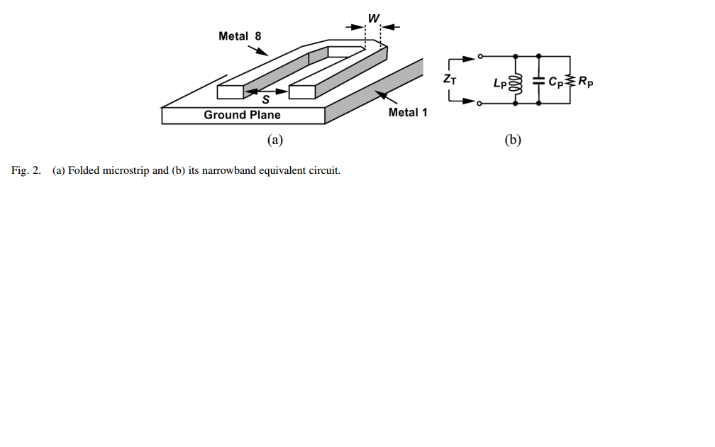
The paper 'A 60-GHz CMOS Receiver Front-End' from Behzad Razavi, it said that he uses the metal to form the microstrip line.
As in the bellowing figure, I am confused that in the chip layout, the metal 8 and metal 1 are far away, while in his figure, the metal 1 and metal 8 are touched together like a microstrip line.
How does the layout in the chip can achieve this by making metal 1 and metal 8 are connected together? Anyone has ideas?
Thanks.

metal8 is for signal, metal 1 is for GND, no substrate between them?
There should be a complex substrate between M1 and M8 but the author ignored to show the details in his figure in order to simplify it.
Oh, perhaps it has some material between them. Thank you for mention it. I will check.
_how design_LNA MMIC 相关文章:
- Why microtrip T-junction does not show strong reflections similar to 90° bend line?
- Why all phase monopulse examples show parallel beams arriving at antennas?
- How to showing farfield of 2 or more antennas in CST MWS?
- HFSS 3D polar plot does not show up
- Network Analyzer shows positive S11 on passive PCB
- LNA Design - Unable to get Gain from the circuit
