impact of output imaginary impedance on phase modulation
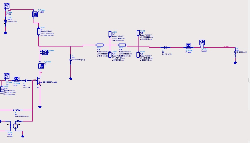
I have designed a class-E power amplifier. To filter usable band (2.2GHz-2.3GHz) I have used 4 open stub to be short circuit at 4 harmonics. Its output impedance is 52+j166. Because my filter and PA work great, I do not want to change my filter or my circuit. But, the point is that its imaginary of output impedance is high and the modulation on this power amplifier is DQPSK. I want to know whether its imaginary part will create some reflected waves and will distort my circuit or not?
If it affects data on modulation, how can I add a matching network in a way that It does not affect the work of my filter and load power?

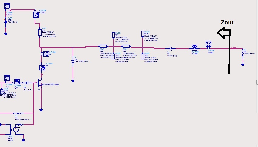
Output Impedance of what?
Of the ampifier?
Yes. It is here:

This is Output Impedance of the amplifier and it should be matched to 50 Ohm to get the Delivered Maximum Power.Nevertheless it doesn't impact the modulation scheme but delivered power is droped if matching is not done.
When all power does not transfer to the load because of an unmatched load, it is losing in a place in my circuit. Where? and how? So, if we look at the circuit in aspect of emitted and reflected waves, will not these waves (the ones which produced lost power because of unmatched load) return to the transistor as reflected waves?
I have another question too (You know lots of things in RF! ). As I said, I have put 4 (the vertical ones) open stubs which their electrical length are 90 degree at second, third, forth and fifth harmonics. The other two Tlines have 50 Ohm. It means that their width is 1.77mm (Rogers Ro4003 at 2.3 GHz, 50 Ohm). The point is when I remove 4 open stubs, everywhere in my circuit has a 50 Ohm impedance, but when I use these 4 open stubs, 50 Ohm impedance does not happen. As we know 50 Ohm impedance should be happened to remove reflective wave and force VSWR to be 1. What should I do? My circuit needs these 4 stubs because they are filtering, but VSWR is important too.
You can not learn everything by always asking questions.You should study by yourself to improve your "taking decision/judgement mechanism".
Yeah, I know, but because I have not fabricated any RF circuit before, I am a little worried about my measurement result!
Since you have already calculated the XL =+166, all you need to do is add an impedance of XC= -166. No ?
At 2.25GHz, you have an L ~ 0.117nH. So you need to add C~ 0.43pF
How you would do this practically is beyond me
However I also notice that the o/p R is 52, and not 50. You can design a matching LC for this too, but the VSWR would be quite low even without it.
I appreciate for your response; however, I want to design my circuit by Microstrip-lines not L/C s. Instead of using a capacitor with 0.43pf I can use two open stubs with Lamda/4 at 2.25Ghz and tune its Z0, but this job will decrease power and efficiency of my circuit. It is because it affects amount of Cs which is responsible for working circuit in class-E PA.
Doesn't the distributed impedance matching network have sufficient degree of freedom to achieve optimal output impedance for class E both for fundamental and harmonics? According to literature, it's possible even for a larger bandwidth, as e.g. discussed in this IEEE paper reprinted by Cree:
http://www.cree.com/~/media/Files/Cr...g_Networks.pdf
An ideal class E amplifier has a pure reactive output impedance, transistor rdson and matching network losses are creating a real impedance. If you perform load pulling, you'll end up with a near 50 ohm real impedance looking into the matching network. The fact that you have a large reactive component contradicts somehow the claim of "PA work great". At least it doesn't work at maximum output power.
If you already achieved the intended output power with the present matching, you'll either accept the mismatch or reduce Vdd and redo the matching.
Dear FvM,
First of all, I appreciate for your response.
Second of all, I have read the paper you have proposed. By this approach (first, load pull analysis, second, obtaining a matching network by L/C s to convert needed impedance (from load pull analysis) to 50 Ohm (load) and third, converting these components to micro-strip lines) I could not find the best power and filtering. For example by load pull analysis I have gained 5.2+J5.4 as the best load for my PA, but when I try to convert it to 50 Ohm by the low pass matching impedance (Chebyshev) presented in the paper presented by you, the structure in the reading cannot give me 50 Ohm at output and its efficiency and power is not good. So, I tried to use open stubs and the other two stubs by the way in this paper: D.Milosevic, J.Tang.Roermund, 'A High-Efficiency HBT-based Class-E Power Amplifier for 2 GHz', 13th GAAS, PAris, 2005. P.P. 46 (the paragraph under figure 4)
It is true that the approach is a result of the way you have proposed in your post and a result of this paper: A.Wilkinson,J. K. A.Everard, "Transmission-Line Load-Network Topology for Class-E Power Amplifiers", IEEE TRANSACTIONS ON MICROWAVE THEORY AND TECHNIQUES, VOL. 49, NO. 6, JUNE 2001, P.P.1204 (the paragraph under figure 4), but it does not need any converting L/C s components to microstrip-lines. Besides it is more decisive and comfortable. I mean it just needs to use 4 open stubs in 4 harmonics and tune the other two stubs to give the best power and efficiency in output.
Additionally, When I say its results is great not only are power and efficiency important for me, but also linearity and a good figure of switch voltage and current are imperative. What's more, the switch voltage and current should not be negative. I can design a class-E power amplifier with 90% efficiency and 35w power;however, the switch current in a period has negative current in some parts. I have seen lots of papers which have negative switch current when they are working as class-E power amplifier, but because I have not found yet how and why switch current can be negative, I can not use a negative switch current in my project. So, I should accept a lower efficiency and power, but I know what is happening in my circuit. These are reasons why I say my circuit work great!
imaginary impact impedance 相关文章:
- imaginary characteristic impedance
- Metamaterials: imaginary part of permittivity being negative
- Impact of S22 on the FoM of an Rf Power Amplifier
- Impact of coupling variation (of Hybrid coupler) in communication system
- Need List of Impact Factor Journals without Submission Fee
- Output Impedance Of a Triple cascode
