Help need for obtaining EM Co-Simulation for 1GHz LNA design in ADS2011.10
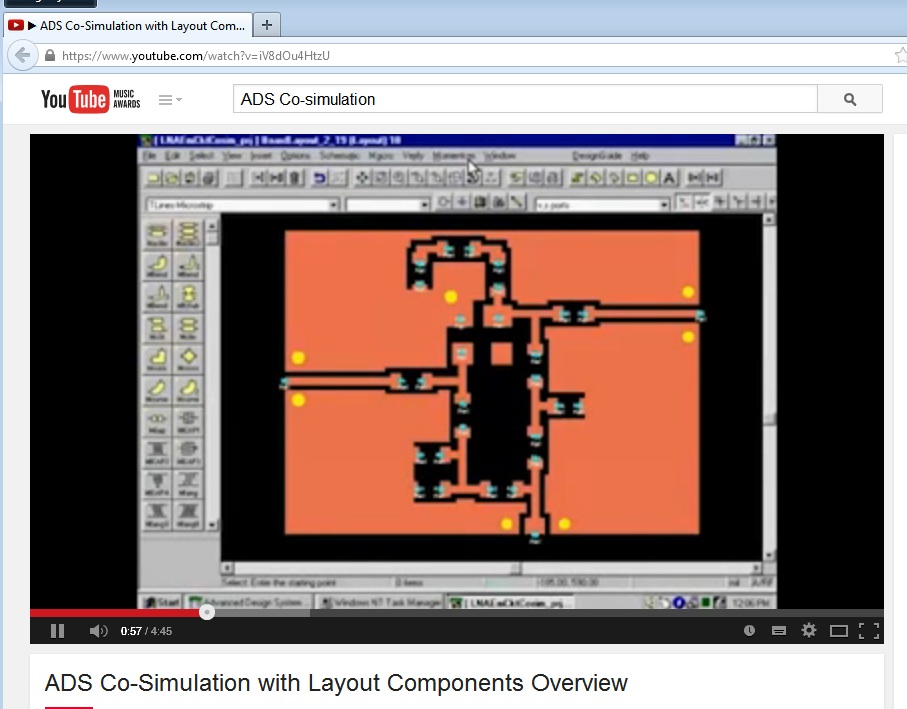
This is example for the layout design of 1 GHz Low Noise Amplifier ( LNA ). This 1GHz LNA, which contains both active( transistors), passive elements(R,L,C), and MLINS. From this schematic, we can generate the Layout of LNA.
My question is, how to get the EM - Co Simulation for this 1GHz LNA schematic circuit. Can you anybody help me to get the EM -Co Simulation for this circuit.
Can you give guidelines, how to get the EM- Co-Simulation, when circuit is built for generating layout, which contains both passive and active elements.
First, you should create its layout with distributed elements in the schematic.Then you have to place the ports for lumped elements ( input and output ports,capacitors,resistors,transistors etc).After that you do a EM simulation carefully in Momentum ( pay attention for ports,meshing,frequency etc) and when EM simulation is succesfully terminated you should create a "layout look-like" view of your layout.Then you will able to place this view with appropriate ports in another schematic test-bench and connect other lumped elements to associated ports and finally do ypur simulations.
Thank you for your elaboration explanation. If somebody knows pdf help document of EM Co-Simulation for circuit contains both passive and active elements as I said in the posting #1. Can you show the help document.
It is exactly what BigBoss has mentioned.
But if you're using ADS 2014 or 2015, you'll find there is a "Co-Simulation" selection you can choose in which you don't need to add every port to lumped elements. It is very convenient.
As you said, how to create its layout with distributed elements in the schematic as I have shown 1GHz LNA layout schematic generation circuit in the posting #1. In the posting # 1, I have shown the 1 GHz LNA Schematic layout generation circuit, from this schematic, we can generate the layout with all components (Transistors, R,L,C). How we can create the distribute elements for my circuit as shown in posting #1 and later we can place pins where ever the connections are existing. Can you help me to create distribution element for my circuit as shown in posting # 1.
Can you clarify it.
Already we have created LNA layout with Components. For EM Co-simulation, how we have to generate the LNA layout without components as shown below screen shots from the already existing LNA layout with components.