Planar Spiral Inductor port defination problem
时间:04-05
整理:3721RD
点击:
Hi
I have been trying to simulate the S11 response of this planar circular inductor. It has one glass substrate (brown color), SiO2 layer (red), gold sputtered planar circular inductor and on top of that silicone rubber. I attached an image of this model here. The problem i have been facing are these:
1. In actual measurement i use a SMA male connector whose ground and central wire is connected to two end of spiral inductor. But when i am modeling, i am defining only one port for S11 parameter. Then what is the ground plane connection in simulated model
2. I modeled one port in the face of center of spiral as seen in image. It doesn't start simulation. The error message is this "Waveguide ports must be aligned with Cartesian coordinate planes for the transient solver."
3. Should i use an discrete port or waveguide port?
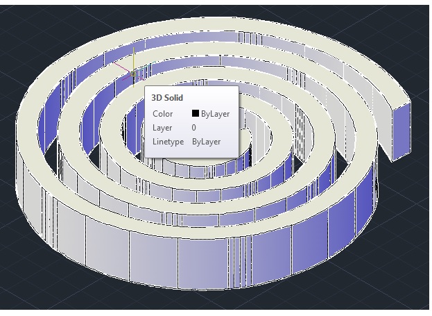
4. The spiral i created here has smooth side on every where. How to create something like this (attached image named proposal)
I have been trying to simulate the S11 response of this planar circular inductor. It has one glass substrate (brown color), SiO2 layer (red), gold sputtered planar circular inductor and on top of that silicone rubber. I attached an image of this model here. The problem i have been facing are these:
1. In actual measurement i use a SMA male connector whose ground and central wire is connected to two end of spiral inductor. But when i am modeling, i am defining only one port for S11 parameter. Then what is the ground plane connection in simulated model
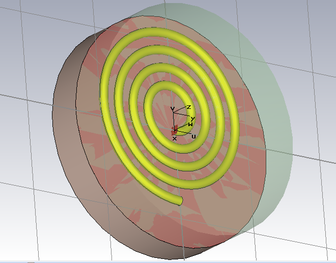
2. I modeled one port in the face of center of spiral as seen in image. It doesn't start simulation. The error message is this "Waveguide ports must be aligned with Cartesian coordinate planes for the transient solver."
3. Should i use an discrete port or waveguide port?
4. The spiral i created here has smooth side on every where. How to create something like this (attached image named proposal)
- Using spiral inductor after SRF
- [ADS] Spiral inductor with SRF below the operating frequency
- [ADS] Spiral inductor parameterization in ADS
- How to calculate Q factor of square spiral coil on substrate?
- log spiral antenna in CST
- In RFIC, spiral inductor behaves as capacitor at some hight frequency . Why so?