CST Background and Boundary Conditions for IC Chip Radiation Sims
时间:04-05
整理:3721RD
点击:
Hi everyone, my first post at Edaboard but have received helps since 5 years ago! I have a serious problem understanding background and boundary conditions in CST Microwave Studio.
I do EM sims for radiating ICs (chips) and sometimes I have semi-infinite Silicon on the back of the chip and I pick up the E-farfield from the semi-infinite Silicon space for avoiding long simulation times when using lens.
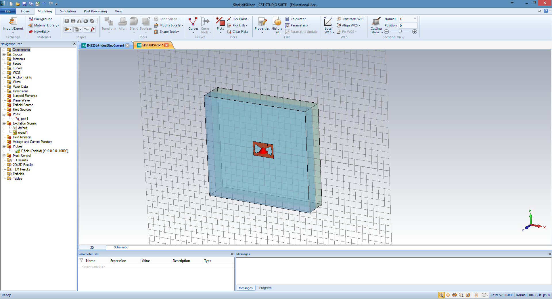
For example, in mentor graphics IE3D, you can define you substrate materials layer by layer. Here, I am confused about the background and boundary definition. Can you please explain these to me? In particular, how can I define this world: half-space air, a 250um thin layer of lossy Silicon substrate, and on the back a half-space of loss-free Silicon. I have attached a figure showing what I have created for now.
Do you have any documents explaining these? I did not find anything having thorough explanation on these two.

Boundary Conditions CST 相关文章:
- HFSS Lumped RLC Boundary
- How to define excitation and boundary condition of a dual and quad output switch?
- Perfect E boundary HFSS
- Meeting oscillation conditions at input or output port gives different matching?
- CST periodic boundary conditions
- CST script - command do not get registered in the history
