Low Noise Amplifier Design at 1.575GHz
In my band of interest the LNA is stable, but i really need to unsure that it is stable for every frequencies?
Thank you.
To ensure a good match , s11 <0.03 or -15dB, not near 1. Shall we guess why?
Sorry, I meant 0dB. I have to ensure that it is under -15dB at my point of operation (1.575GHz)?
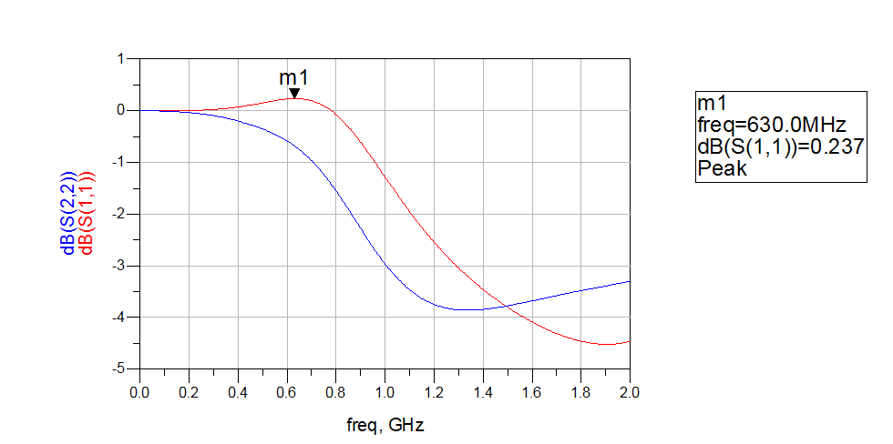
But what is concerning me, is that around 900MHz my S11 is greater that 0 dB..
I changed the polarization, chosen 20mA (less gain) at I get the same situation.. Any ideas?
You amplifier is not stable therefore S11>1 in that band.Check the stability..
But I pick up both matches by doing analysis of the regions of stability. We do that analysis for the frequency of interest.. How can I guarantee that it will remain stable for all other frequencies?
This is what I get after the matching newtworks:

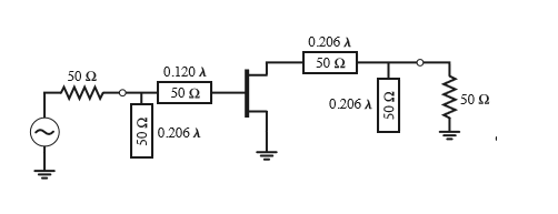
What kind of input and output matching network are you using ? which device ?
I'm using this: http://www.avagotech.com/pages/en/rf...ect/atf-55143/
Matching network is like this one:

You should check the stability by plotting K and Mu stability factors up to fmax. of the transistor.If you see unstable regions, you should check the input and output stability circles for the band(s) of unstablity.Then you have to examine each unstable region and after that you should find and apply a "stabilisation techniques" ( for instance a parallel resistor with a DC blocking capacitor in series at the input/output or an amount of series/parallel frequency selective negative feedback, or simple a high valued resistor between Drain and Gate etc.)
There are many stabilisation techniques but it's essentially to move out the input/output stability circles from Smith Charts active region.
And also, why don't you look at this APP. Note ? It's pretty useful.
http://www.avagotech.com/docs/5988-9555EN
You can try to optimize the circuit in ADS with stability and NF as constraint and microstips parameter as variables
I already accomplished the stability by using some stability techniques in the Gate and Drain of the Transistor; in the regions of the instability I applied resistors to dissipate the power, so that the negative resistence that we would see if we look inside the Drain/Gate would disappear :).
