Help understanding discrete balun and matching network
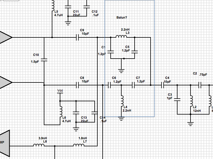
Here's my circuit, and the data sheet says the suggested load impedance should be 12+13j

Now I spiced the section marked balun and I found the top and bottom had a resonance near my frequency of interest, with a phase shift. So I think the purpose of that is to combine the positive and negative into a single ended signal. I struggled to understand what effect this portion had on the impedance.
I think C9 and C8 are just DC blocking caps.
I don't know what C10 does.
I think L5, C11, and C12 are some kind of choke? Not sure why you need DC here.
C4 I think is just another DC blocking cap?
C2,C3,L1,L2 I think are supposed to be the matching network for the antenna although it did not seem to match from 12-13j to 50Ohm. I've considered the idea that this design was tuned and takes into account all the parasitics of the layout but I'm not sure if that's what's throwing me off.
L7,L8,L9,L10,C15 I think are some sort of balanced filter for the RX? I haven't looked into this part yet.
The thing I really can't understand is the impedance of this circuit. Based on the statement that the transmitter wants a load of 12+13j, and the antenna is supposed to be 50Ohms, i thought I could work my way back adding each component to a smith chart (with smith chart tool) and in the end I'd find myself at 12-13J the conjugate of the load impedance they specify. I even tried doubling the values in the differential section to treat them as single ended. No matter what I tried I failed pretty miserably here, and it's quite literally keeping me up and night right now. If anyone would be kind enough to try to help me understand this circuit and put me on the path to higher learning I would really appreciate it. I'm trying to teach myself some things but I hit a wall here.
I was thinking about renting a VNA and just measuring everything but that won't really teach me what's happening. I could try simulating too but still I don't know that would lead to understanding.
The enclosed section resembles a twin-T filter, which usually is bandstop. Both LLC and LCC networks connect to the same output (like a normal twin-T). However their inputs are not directly connected, so your theory is probably more correct than mine.
The discrete balun and output filter combination has several degrees of freedom, one of it is the impedance of the center junction.
One approach is to make the left side performing the impedance transformation so that the right pi filter acts as an additional low pass that can be omitted without changing the impedance matching. (center impedance 50 ohm)
Second approach is to equally distribute the impedance matching job between both networks, probably achieving lower sensitivity to component tolerances. (center impedance e.g. 20 - 30 ohm)
A very important point must be mentioned. You are simulating ideal LC networks. The real component impedance and respective network function with all parasitic elements in effect is a different thing. So you need to master two tasks:
The "discrete balun" theory, allowing you to synthesize a network with intended parameters
VNA measurements to determine the actual impedances and correct component values to achieve the intended behavior
Application circuits with component values are most likely already considering parasitic elements (otherwise they would be useless for 2.4 GHz). So it's probably impossible to verify it in a simulation with ideal parameters. But it's not sure if the application circuit actually reaches an optimum, considered that they have been designed with limited time budget (and possibly even limited RF experience).
I recently did a similar job by redesigning a 915 MHz discrete balun. I found that the published manufacturer application circuit was O.K. in terms of output power and output impedance, but involved a considerable asymmetry, making 2nd harmonic worse than it could be. After optimizing the circuit, a second low-pass filter suggested by the manufacturer could be omitted.
I'm on board with learning "discrete balun" theory. Any suggestion on a reference I should start with?
A bit of theory can be found in application notes, e.g.http://www.ti.com/litv/pdf/swra236a
discrete understanding balun 相关文章:
- Discrete transistors sot343 cascode amplifier
- Which discrete component modelling to use? (S-parameter or Spice)
- Discrete PLL in this oscillator/converter, how does it work?
- CST discrete port for Strip lines?
- Discrete transformerless DBM question
- Discrete Port or Waveguide Port for SIW antenna in CST
