Waveguide slot antenna confusion about radiating and non-radiating slots.
Assume we have TE10 waveguide with slots.
I have some confusion, which comes from here:
1) http://www.radartutorial.eu/06.anten...ntenna.en.html
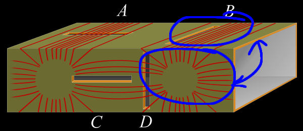
it is written that (slot A) will radiate,
and (slot B) will NOT radiate
2) http://www.antenna-theory.com/antenn...dWaveguide.php
Figure 2. Waveguide with a thin slot centered about its width.
it is written that slot similar to (slot A case 1) will NOT radiate (opposite statement to case 1)
Figure 3. Horizontal slot in a waveguide.
it is written that slot similar to (slot B case 1) will radiate (opposite statement to case 1)
3) http://www.qsl.net/n1bwt/ch7_part1.pdf
explains things a little on page 4:
it seems that radartutorial.eu website waveguide image current distributions are somehow wrongly placed (wide wall current distribution is shown on narrow wall)?
I found an image of slot antenna here: http://cn.comsol.com/model/substrate...-antenna-16021
What is the purpose of small short 90 degree angled slot extensions at both ends of each slot? What is the idea behind this? I did not found such slot configuration in slotted waveguide papers.
as far as the 90 degree ends of the slots in the Comsol example. I would guess the total length of the slot, including the two tabs at the end, is approximately half wavelength, so that it resonates. Then the two 90 degree tabs are coupling energy from the waveguide (near those top edges of the waveguide are maximum current flow points).
It think that you are right about total slot length (including 90 degree parts) and excitation frequency.
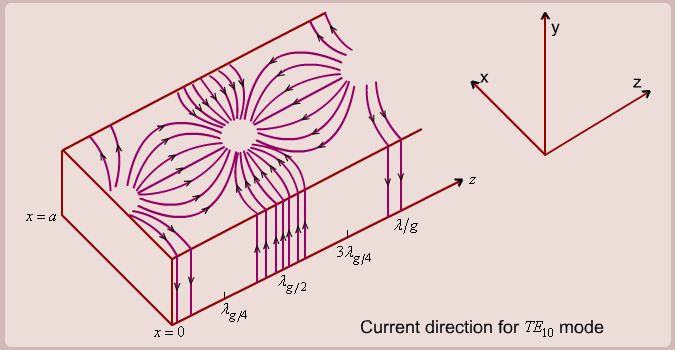
Still not sure about current distribution here (te10 waveguide):

(fig.3 from http://www.radartutorial.eu/06.anten...ntenna.en.html)
and here:

(at the bottom of page http://nptel.ac.in/courses/117101057/Slides-6/7.4.html)
The second image seems to be correct.
I have a new question about SIW (substrate integrated waveguide) to microstrip line taper transition.
There are different formulas to calculate such taper. One approach is to calculate waveguide impedance.
I was given few formulas:
ZTE=Sqrt(MU/E0)*LG/LAMBDA
ZPI=ZTE*Pi^2*B/(8*AS)
where AS is SIW dielectric filled waveguide (DFW) width
(AS formula from http://www.microwaves101.com/encyclo...ated-waveguide)
As i understand, waveguide impedance ZPI then can be used to calculate microstrip line width (connected to SIW). Is it correct?
To clarify:
50 ohm microstrip - > quarterwave transformet to ZPI -> ZPI of SIW waveguide
50 ohm microstrip - > taper from 50 Ohm to ZPI -> ZPI of SIW waveguide
or ZPI can't be used in such way?
How one can measure conductance of slot, and what equipment is required?
Also, how to measure conductance of slot in simulation?
Formulas exists to calculate slot conductance, how we can practically measure it?
I think we can use two identical waveguides. One with slot, and one without slot.
Measuring S11 and S21 of waveguide we can find variation and be sure that loss in s21 power is not due to reflection (s11). I mean if S11 not changed alot, or become better, and s s21 becomed smaller, then difference is radiated, but also maybe dissipated in heat.
