Impedance discontinuity on SMA connector
My design works up to 4 GHz.
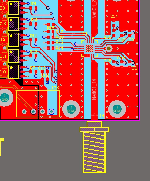
As shown in the attached pic, I have an SMA connector soldered to the board.

The track width is 0.5 mm as the connector pin diameter is 1 mm roughly.
There will be impedance discontinuity due to this difference between the track width and the connector?
Thanks,
Jose
Sure, but why is your trace so thin? The impedance of the trace should be near 100 Ohm but your SMA has something near 50 Ohm.
Hi John.
I made the calculations as shown below


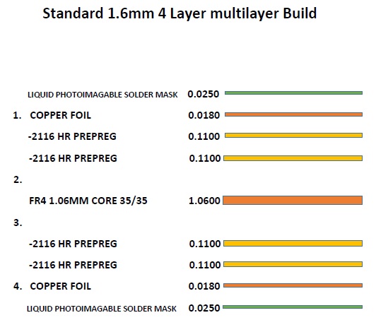
The pcb manufacturer specs give an Er of 4.38 at 1 GHz. My layer stack looks like this:
SIGNAL
GND
POWER
SIGNAL
Did I do anything wrong?
I am a bit newbie with RF design.
Regards
i hope this will help you understand the transition from coax to CPW.
http://www.artechhouse.com/uploads/p...n_941_CH04.pdf
In addition to the shunt capacitance, you might also have some series inductance in the ground connection from SMA ground to PCB ground.
Knowing the values of these parasitics, you can usually compensate them. For example the shunt capacitance, you can add a series inductance towards the circuit, followed by another shunt capacitor. This will form a low pass where the shunt C parasitic is the lowpass C.
most likely, but there's going to be a bigger discontinuity due to the incorrect method of SMA termination to the board
you need to have a close read of that article link in post #4 by rizwan
that looks like a good book!
Verify your dielectric constant above 1GHz and loss tangent. e decreases to 4 and loss tangent increases with f and may be poor. CHeck there are many types of FR4 such as Polyamide. (hint)
Note 50R is ~ 2:1 for Width to Height above ground plane, for e=4.3 affects choice of board thickness.
Choose an edge mount connector with gnd pins and std board thickness to match. track to pin size.
Your SMA looks like vertical, not edge mount.
AS a result your Return Loss will be very poor.
Hi again guys.
Thanks for all the responses.
I had a look at the document suggested by rizwan183. Now I understand a bit more about this.
Finally, I am using a different pcb manufacturer and placed GND plane in a different layer so now I can have a wide enough track without width changes, as shown in the pics.
Now my layer stack is:
SIGNAL
--------
GND
SIGNAL+POWER


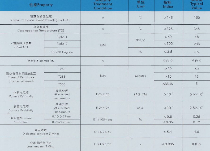
These are FR4 specs. How should I use loss tangent?

The SMA I used is this one:
http://uk.farnell.com/te-connectivit...ohm/dp/1056375
The signal return path is through mounting holes and chassis. Is that way not good?
I have seen it in splitters and other L-Band stuff.
As volker@muehlhaus mentioned, the ground path through case and ground plane contact creates a series inductance. I would expect a bottom ground plane, galvanically and/or capacitively coupling to the case surface. Surely not as good as an edge mounted SMA.
No specification in the FR4 datasheet is valid for 4 GHz. If you want to include dielectric losses in a simulation, you should refer to FR4 loss curves in literature.
My comments stand.
Straight Bulkhead Jack = Wrong connector for EDGE layout,
pcb DESIGN = wrong impedance control of traces,
fr4= wrong material for anything WITH NO SPECS of D vs F above 1`GHz
back to the drawing board..
Hi SunnySkyguy
Could you be more specific with this?
Is it because dielectric specs?
Characteristic impedance is always governed by the "effective ratios" of signal to ground radius and effective dielectric constant.
They must be match on both sides of an interface.
This results in ratio of the distributed capacitance and inductance that increases by area or R^2 so that Zo is proportional to the sq.rt of L/C.
Thus when having a huge discontinuity between coaxial shield/signal pin radius with the PCB signal track (and also different dielectrics at the interface), you can't avoid fringe effects with of mismatched impedance at the interface. I
f the board has a coplanar ground track that lines up with the connector coplanar mounting tabs ( which bulkhead do not) and the signal trace width matched the connector pin width, you would have no discontinuity and fring3e effects. that affect Return Loss
Thus the board design is no good.
The same problem exists if a coaxial connector is pinched with a discontinuity or a coaxial braid is not terminated correctly. due to the imperfections at that interface causing a poor controlled impedance.
The board must match the connector geometry, like any waveguide.
in this case , wrong connector., since it has no ground tabs for extending the geometry to the board
Start the design by specifying your tolerances for Insertion Loss and Return Loss over desired BW and budget .
Then specify your tolerances and deviations of dielectric constants which vary from dielectric types and frequency @>= 1GHz
( Getek is OK at 1GHz but not 5) So research on all dielectric types is a must for cost vs performance. There are dozens of material options ) Consider Board shop TDR testing S ( waste area test tracks) for adjusting trace widths to compensate for 10~20 variation in dielectric constant.
then restart design or accept as is.
Don't want to contradict SunnySkyguy in general.
I believe that both microstrip calculations for 0.2 mm and 1 mm substrate height are basically correct, variation of FR4 permittivity and losses are points to consider, but FR4 is still used for consumer WiFi equipment at 2.4 and even 5.7 GHz. Just a cost versus perfomance trade-off.
Ground discontinuity with the bulkhead jack is a fact, acceptability depends on your requirements which haven't been stated.
Yes but for newbies it is important to remember that FR4 just means the epoxy fiberglass has additives for a Fire Retardant rating of FR4 and has nothing to do with dielectric constant or loss tangent. Historically it means it is lossy for microwave, but in the last 20 years many new offerings exist other than teflon= that proviude a compromise to price and performance.
There are dozens of material types with different ratios of epoxy to fiber glass and polyamide.
Never assume . Always get the vendor material specs for this.
The board itself is an L-Band attenuator based on Mini-Circuits DAT31R5A-PP+ IC.
Its purpose is allowing the user set beacon signal attenuation level for satellite tracking.
The resolution of the system should be 0.5 dB but 1 dB could be acceptable.
The input signal comes from a block down converter and the output is connected to an antenna control unit.
I forgot to mention...it will really work up to 2 GHz, not 4.
Thanks for the support guys
Agreed. SunnySkyguy likes simple generic statements, and ignored that you have a simple thru line. You wouldn't want to built any resonators on FR4 that need high Q, but thru lines are OK if you can accept the extra insertion loss.
Regarding the SMA, I assume that it's a symbol picture only, and you have assured good grounding with minimum path length?
The idea was using the pillars fixing the board to the chassis as the return path. That is why I placed the mounting holes close to SMA's.
As the board hasn't components at the bottom, I guess I should discard pillars.
Am I right?
Looks bad to me. You need real good short path ground, designed with similar care as the signal line. The effect of any length is the ground is just as bad as any length in the signal line.
If your board is placed inside a metal box and the coax shield is screwed into/soldered onto the box and your board ground frame is well connected (=short path) to the box, that would be an option. Microwave PCB often do that, with PCB ground flat on metal box rim, carefully connected over the entire PCB outline.
But if you have solder resist on the PCB backside, and need to go through mounting holdes at some distance, that won't work. In this case, better use SMA with ground pins soldered directly to the PCB ground.
I found out that prototyping is very useful in such cases. Just order PCB with several trace widths, ground soldering layout.
SMA <========= microstrip line 1============> SMA
SMA <========= microstrip line 2============> SMA
SMA <========= microstrip line 3============> SMA
SMA <========= microstrip line...============> SMA
SMA <========= microstrip line 10============> SMA <- calculated width (expected to be best)
SMA <========= microstrip line...============> SMA
SMA <========= microstrip line 19 ===========> SMA different solder layout
SMA <========= microstrip line 20===========> SMA different solder layout
then you can use SMA connectors/cables to connect each of microstrip lines to your main PCB. If there any significant difference you will notice that. It can be done without any measurement devices, just use your main PCB output (signal strength, etc.) to see changes. Then you can draw graph, see tendencies, and even produce new prototype test board with narrower width step, or layout styles.
I used such prototype to test quarterwave stubs, radial stubs.
discontinuity Impedance connector 相关文章:
- which type of impedance discontinuity is worse (picture)?
- Output Impedance Of a Triple cascode
- How to make image impedance equal
- Input and output impedance matching in Distributed amplifier
- Characteristic impedance of combination of CPWG and stripline on inner layers
- Problem of impedance matching of Gilbert cell mixer
