RF phase shifter design/optimization in ADS
时间:04-04
整理:3721RD
点击:
Hello everyone,
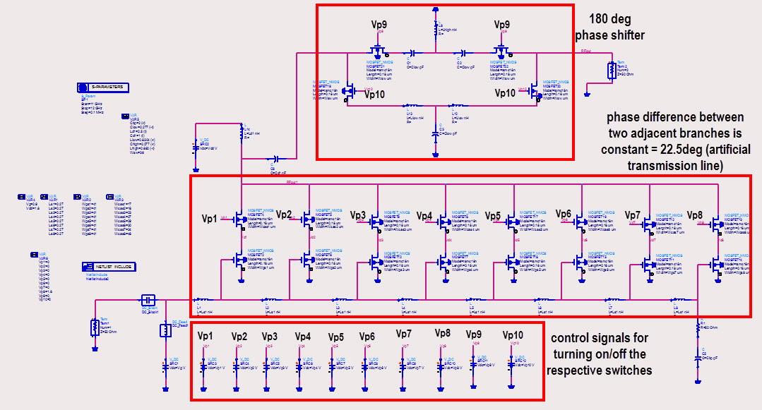
Schematic Description
I am designing RF phase shifter in ADS at 11-12GHz for a beamformer (rf phase shifting topology). The schematic can be seen in the attached image file. As you can see, it's a combination of a 3-bit distributed phase shifter (The Cgs capacitances of the bottom nmos transistors in each branch combined whith the inductances Ls compromise an artificial transmission line with characteristic impedanse Z0=sqrt(Ls/Cgs) and constant phase shift Dph=ω*sqrt(Ls*Cgs)) and an 180 deg phase shifter.
This topology allows to vary the phase from 0deg to 360deg in steps of 22.5deg.
Question
After first design pass, the circuit is functional but it needs optimization.
When the first switch is on and all others off (Vp1=1.8, Vp2=...Vp8=0) then the phase of S21 is 0, Phase_S21_vp1=0deg.
- (Vp1=0, Vp2=1.8, Vp3=...Vp8=0) -> Phase_S21_vp1=22.5deg
- (Vp1=0=Vp2=0, Vp3=1.8, Vp4=...Vp8=0) -> Phase_S21_vp2=45deg
.
.
.
- (Vp1=...Vp7=0, Vp8=1.8) -> Phase_S21_vp8=157.5deg
How can i make this kind of sweep, where the switches are turned on sequantialy and at each step only one switch is on while all the others are off.
Also as i understand, i have to optimize 8 parameters (Phase_S21_vpi, i=1,...8.).
Any suggestions and ideas about how to set up the sweep and optimization plan in ADS would be very helpful.
Thank you in advance and sorry for long post.

I have found solution for my problem.
The way to do the kind of sweep that i asked previously is to use the BATCH SIMULATION component in ADS. More info can be found in example located in folder:
\Agilent_ADS\examples\Tutorial\BatchSim_Example1_w rk.7zap
Regards, Alex.
