[Moved] Design of Low Noise Amplifier


Have you ever checked the DC Operating Point of the MOS transistors ? I think they don't work because the Bulks are not connected to nowhere.
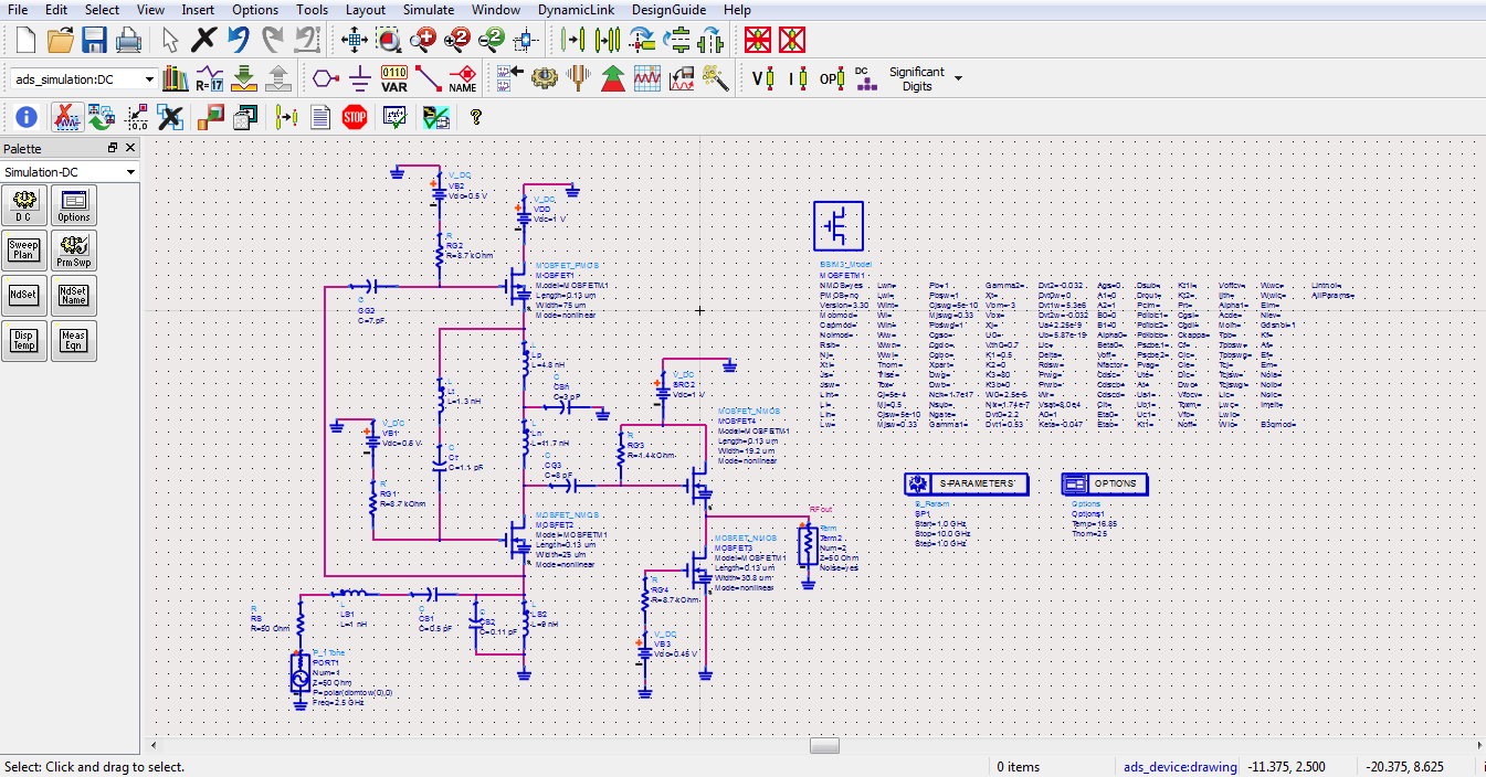
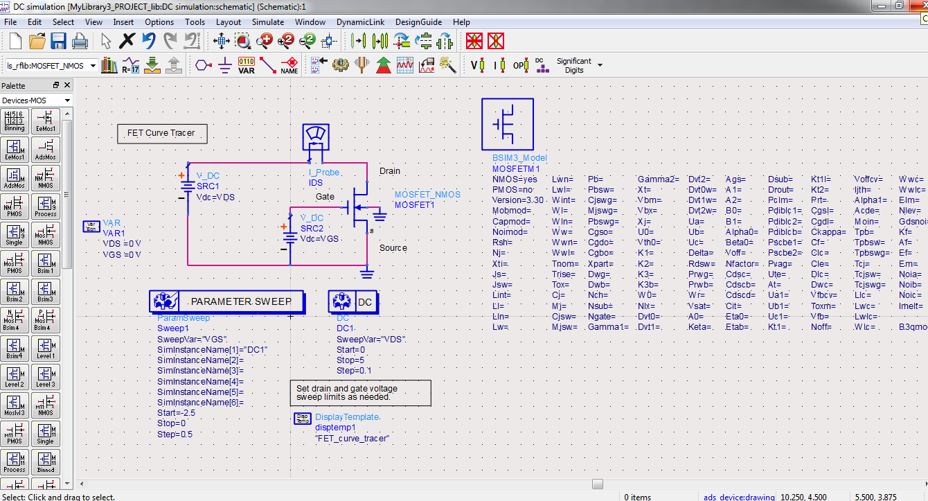
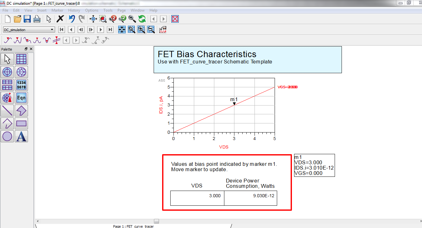
We checked DC operating point using both DC annotation and FET curve tracer but we got different values.How do we use these values in LNA schematic in order to get postive gain.
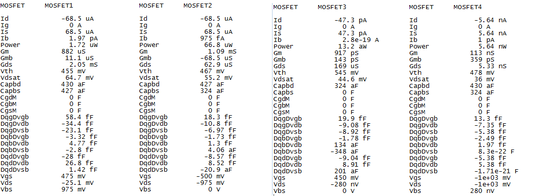

MOS 3 is totally off :) pA !
you connected the gate voltage of MOSFET4 to negative voltage !
I do not understand your biasing circuit.
we have made the changes in circuit schematic and simulated.we biased the transistor and used these values in schematic but even then the gain is negative can you suggest some 130nm transistor model.


We did check the DC operating point and simulated the schematic and still are getting negative gain. Have we used the bias characteristics value correctly ? If not how do we do it ?
Attachment 127845Attachment 127846Attachment 127847Attachment 127848
as I see here TM2 is PMOS and TM1 is NMOS. You have to use TM2 on top not TM1
are u using noise cancellation technique ?
this is
