Problems with substrate contact layout using IBM8HP
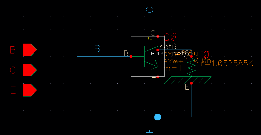
I was trying to draw a layout for a simple NPN in IBM8HP. Below is the schematic:

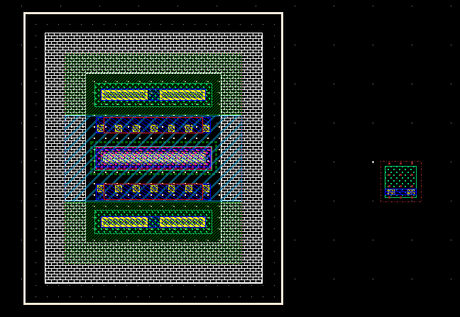
I used the "subc" as a contact to the substrate, which was provided by the PDK in the schematic. However, I don't know how to connect this "subc" in the layout!

I didn't find the bulk terminal in the layout of the npn, but this bulk terminal appears in the schematic.
Could anybody please help?
Thank you very very very much!
Didn't Virtuoso Layout XL show the connections as rubber-bands ?
Thank you so so so much for your reply!
No! I've tried to use the Virtuoso Layout XL in order to find some hints, but none was given.
There's another problem I am worrying about: Is it better for the substrate contact to form a guard ring in the layout? If so, I have to take the width and length of the substrate contact into consideration when designing the schematic, because I have to set the width and length of the "subc" symbol before placing it onto the schematic. I think it is hard for me to make sure what the length and width of the substrate contact would be before working on the layout of the whole circuit. :(
substrate Problems contact 相关文章:
- Antenna design with 'Air Substrate'
- Ceramic or High K PTFE Substrate
- How to mount RF substrate into a Al housing for making an RF module
- best MS substrate to use in a wireless energy harvesting (rectenna)
- Substrate to substrate interconnect between two CPW substrates
- How to choose the substrate's thickness for a 9.35Ghz application
