Help with RF High power amplifier (53 dBm).
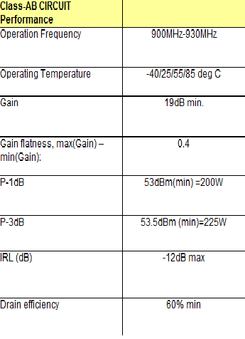
Let me define target specs before I go into the problem.
So, according to the device load pull data I selected the optimum Z_L = 2.01+j*0.85 which meets the target specs.
Z_s =0.65-j*2.75 (Source impedance).
I am attaching the complete the BOM +layout. Please, see below

Below are the measurement results,
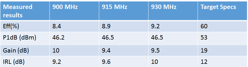
There is not much of a correlation between my simulation results and measurement. Loss of 6 dBm output power is way too much.
Any help would be great.
P.S,
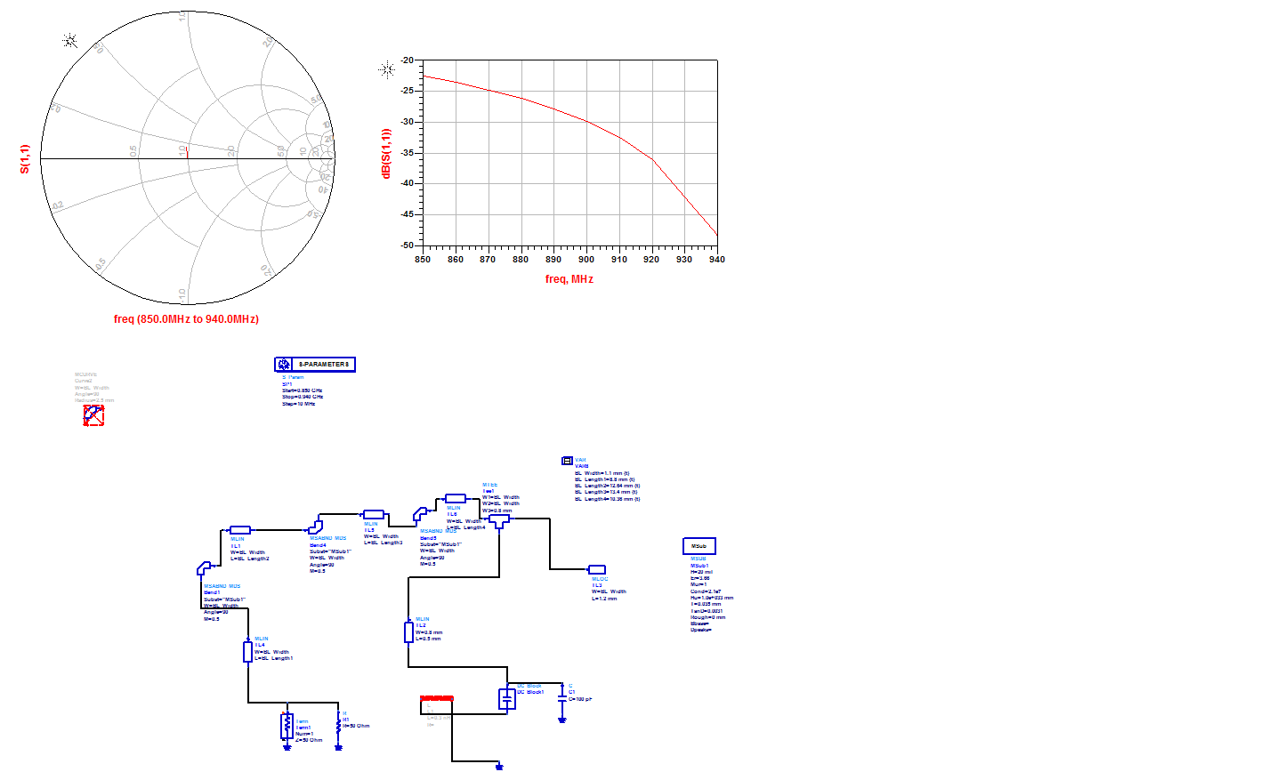
Down below are simulated results,

OMN total PCB length------------> ~28 mm(I am a bit skeptical about the length though)
IMN total PCB length------------> ~65 mm
Thanks
I presume you refer to datasheet specifications rather than actual load pull? Means you know effectively nothing about the matching achieved in your hardware design, except for simulation results?
The customer has given us the actual load pull data at 915 MHz. Since, it's a narrow band design I assumed there wouldn't be a great jump in the impedances.
As with all high power RF MOSFET amplifiers, there's a large impedance ratio to be matched. Seriously, I won't believe a single number claimed about the design if it hasn't been empirically verified with the actual design.
The gain and power numbers suggest that the intended matching hasn't been achieved, or there's another design property which differs considerably from the datesheet reference design.
Well, ofcourse there is a large impedance ratio. I don't understand what you mean by empirically verified with actual design?
Yes, I agree that the impedances are way off. But the simulation says otherwise. To debug this problem I can only simulate and see where I am going wrong. But since there is no starting point what so ever I am descending into anarchy.
There's no measurement of actual impedances, respectively S11 and S22. You don't know how the matching is wrong.
If you look at the table in the OP I have S11 at -10 dB flat throughout the band. Measuring S22 is quite delicate. I will have to change my set up.
I'm not sure the problem is only due to matching. However the datasheet (pag. 8) gives a load-pull impedance (max Pout) of 0.97-4.5j at the input and 2.04-0.34j at a frequency of 960 MHz. Even if you have a lower frequency these parameters seems to me too far from yours.
Are you sure the Vgate and Vdrain tracks are correct ? at a glance the seems a little by thick (but I maybe wrong). However you could try to put in series an inductor to increase their impedance unless they are part of the impedance matching.
I read just now the transistor (PTVA102001EA) works in a band 960-1400 MHz. You are below.
They also did a LP analysis on 915 MHz, Max Pout = 54.31 dBm @ 2.10-j*0.08 at the output.
And at the input it's 0.61-j* 2.75(No info other than that at the input side).
For bias lines, I just used a 50 Ohm line corresponding to RO4350, 20 mils which is 1.1 mm in width. Usually, the input side is even more thinner than the output side because of obvious reasons. I just re-used it for the input as well. (May be that's causing a high resistance thereby losing some power, not sure though)
I will try adding a series inductances. In my simulation adding a series inductances at the output gives a much better return loss for the bias lines. But even before the series inductance the S11 for the Output bias lines were much better.
PFA,