design a Substrate integrated waveguide, help!
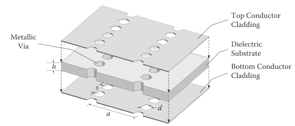
I would like to simulate a SIW using CST but I have some confusions such as , do the vias should be substracted only from the substract ? if I do so I can't see the vias they just disappear as in figure1, if I am doing things wrong please correct me. My second question is how to get the same structure as in figure2 , knowing that if I substract the vias from the upper conductor they just appear in the upper conductor without any extension into the substract and the bottom conductor. the same if I substract from the other parts it just appear within the concerned part and not as shown in figure2. please help!


I never used CST, but i can give you a hint: vias can be filled with metal, result will be the same.
But i think you just need to find some tutorial or example with vias.
I tried SIWs in Sonnet Lite, vias are made very easy, S11 results for SIW resonator was similar to paper i read. If you need fast result and see how things work i would recommend Sonnet Lite.
thank you for your reply! I couldn't found a tutorial about designing SIW so after giving up I used a trial and error method and I have found out how to do it.
could you recommend me any paper so I can compare the results of the simulation.
thank you!
This one for example: http://esss.com.br/events/ansys2010/pdf/22_6_1230.pdf
"FR-4 Substrate Integrated Waveguide PCB at 20GHz". But also many of them.
there are many papers, google for:
"substrate integrated waveguide design filetype:pdf"
put in in google without (")
