微波EDA网,见证研发工程师的成长!
首页 > 研发问答 > 微波和射频技术 > 天线设计和射频技术 > (Understanding) Problem: Load-Pull in Cadence/Virtuoso

(Understanding) Problem: Load-Pull in Cadence/Virtuoso

时间:04-04 整理:3721RD 点击:
Hi,

if I understand this right, then Load-Pull means, that a load with a tunable impedance is connected to the output of a circuit (for example an amplifier). Then this impedance is varied and the power which is delivered to this load is observed. If this power is at its maximum, the corresponding impedance is the complex conjugated of the output-impedance of the actual circuit (the amplifier). Is this right?

The same method should work to find the input-impedance of a circuit (Source-Pull?).

I read in the "SpectreRf Workshop" PDF about "Power Amplifier Design Using SpectreRf" the chapter about "Load-Pull Measurements". I simulated the example circuit and everything was fine.

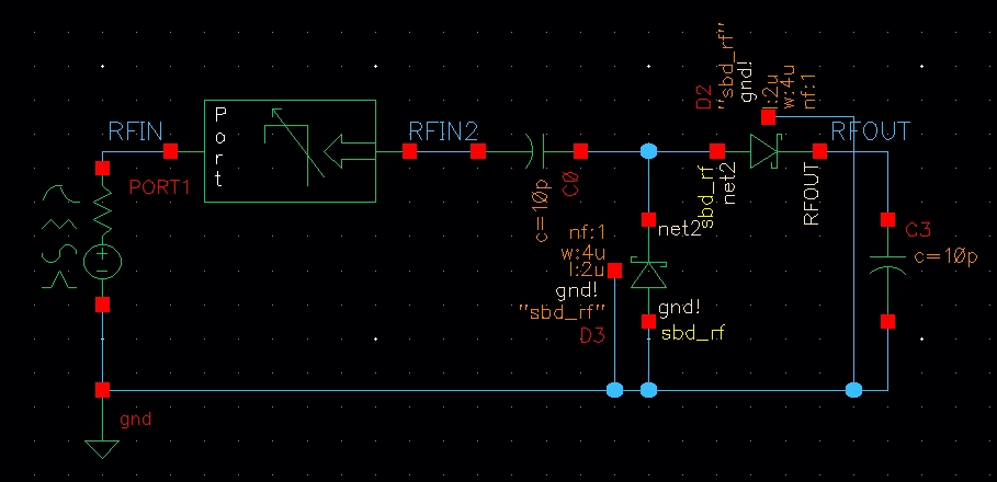
My goal is to find the input-impedance of a simple rectifier (the impedance, at which the output-DC-voltage is at its maximum).
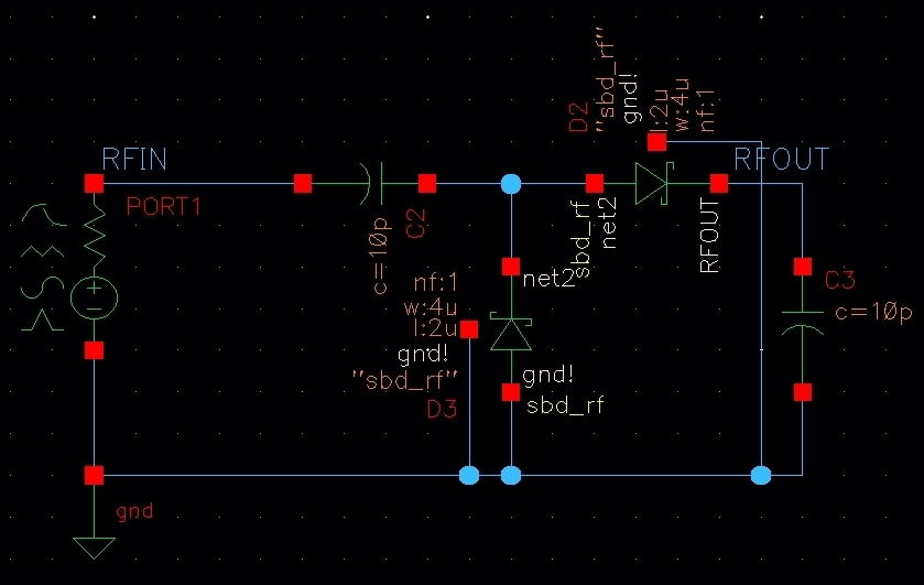


This is the analyses form:


And this is the properties form of the port:


The variables:


If I do a normal hb- oder pss-simulation (normal means: no load-pull) the simulation results are as expected.


But with activated load-pull, the port delivers always 0 W (RFIN is in the order of E-171 V).
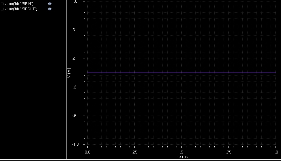


What am I doing wrong?
I tested this with only an inductor instead of the rectifier. Same result: without load-pull everything is fine, with load-pull everything is zero.

Additional question: Can anyone explain me, why I have to fill in 50 Ohm? At 3 places: Z0 in the analyses form, resistance in the port-properties, r0 in the variables. I thougt, that the impedance is varied. But where are these 50 Ohms used?

Please help me!
Thank you!
Sascha

Right.

Correct.

Show me Spectre's netlist.

If you don't use r0, you don't have to define r0 as design variable.
As far as you do load-pull correctly, resistance in the port-properties will be ignored.
Z0 in the analyses form is actually used in Z0 in load-pull analysis.

The impedance which you have found by applying Load-Pull technique is NOT the complex conjugate of the output impedance of actual circuit.Optimum impedance is generally pretty different than complex conjugate of the output impedance of the circuit.Load Pull technique is very useful for Power Amplifiers and it's generally measured and simulations are pretty far from the reality due to model inconsistencies,uncertainties and rough model approximations.

I guess you're trying to find Input and Output Impedances under large signal conditions.In order to do this, you may try some simulation techniques such as PSS, HB or LSSP.They will give you a right aspect for your circuit.

Code dot - [expand]
1
2
3
4
5
6
7
8
9
10
11
12
13
14
15
16
17
18
19
20
21
22
23
24
25
26
27
28
29
30
31
32
33
34
35
36
37
38
39
// Generated for: spectre
// Generated on: Jul 20 11:10:32 2016
// Design library name: RFworkshop
// Design cell name: EF_example_loadpull
// Design view name: schematic
simulator lang=spectre
global 0
parameters pin=0 fin=1G theta=0 r0=50 mag=316.7m
include "/data/wms_hf_u/ghz_rfid/v2/cadence/TECH/tsmcN90rf//../models/spectre/toplevel.scs" section=tt_lib
include "/homes/lischer/diode.scs"
 
// Library name: RFworkshop
// Cell name: EF_example_loadpull
// View name: schematic
C4 (net2 RFIN) capacitor c=10p
C5 (RFOUT 0) capacitor c=10p
D5 (net2 RFOUT 0) sbd_rf w=4u l=2u nf=1 m=1
D4 (0 net2 0) sbd_rf w=4u l=2u nf=1 m=1
PORT1 (RFIN 0) port r=50 num=1 type=sine freq=fin dbm=pin fundname="RF"
simulatorOptions options reltol=1e-3 vabstol=1e-6 iabstol=1e-12 temp=27 \
    tnom=27 scalem=1.0 scale=1.0 gmin=1e-12 rforce=1 maxnotes=5 maxwarns=5 \
    digits=5 cols=80 pivrel=1e-3 sensfile="../psf/sens.output" \
    checklimitdest=psf 
lphb  loadpull  inst=PORT1  rho=mag  rhostart=0  rhostop=990m
+     rhostep=110m  phi=theta  phistart=-180  phistop=160  phistep=20
+     z0=50  {
  hb  hb  autoharms=yes  autotstab=yes  oversample=[1]
+   fundfreqs=[(1G)]  maxharms=[5]  errpreset=conservative  annotate=status
 
}
 
modelParameter info what=models where=rawfile
element info what=inst where=rawfile
outputParameter info what=output where=rawfile
designParamVals info what=parameters where=rawfile
primitives info what=primitives where=rawfile
subckts info what=subckts  where=rawfile
save PORT1:p RFIN RFOUT 
saveOptions options save=allpub currents=all

The r0 variable was defined in the SpectreRf Workshop Example. It is indeed unnecessary.

This I don't understand. Where is this Z0 needed during the load-pull simulation? Is it maybe only needed as scaling factor for the smith-charts?


I have to design a rectifier which acts as power source for a RFID-Transponder. The circuit in the picture in my first post was a simplification. Until now I used pss-simulations and different calculations to determine the impedance of the rectifier. For example Ohm's law:

harmonic(((-1 * vh('pss "/port0_plus")) / ih('pss "/PORT0/PLUS")) 1)

Or I used the magnitudes and phases of the input voltage and current:

complex(((ymax(vtime('pss "/port0_plus")) / ymax((-1 * itime('pss "/PORT0/PLUS")))) * cos((harmonic((phaseRad(vh('pss "/port0_plus")) - phaseRad(ih('pss "/PORT0/PLUS"))) 1) + pi))) ((ymax(vtime('pss "/port0_plus")) / ymax((-1 * itime('pss "/PORT0/PLUS")))) * sin((harmonic((phaseRad(vh('pss "/port0_plus")) - phaseRad(ih('pss "/PORT0/PLUS"))) 1) + pi))))

The impedance value is needed to design an antenna for the RFID-Transponder. But I think, that a impedance matched system is not optimal. A larger R in the antenna results in a larger voltage amplitude, which is better for the diodes. I want to test, if this leads to an higher DC-Voltage at the output of the rectifier. I tried to use a simple variable sweep to run pss-simulations with different R-values. But many of these simulations didn't run because of converge problems. Therefore I thought, that the load-pull-method is better to simulate the rectifier with different impedances in the port (which acts as an equivalent for the antenna).
I hope you understand what I am trying to say (sorry for my bad english)!


I have an additional question:
In the "SpectreRf Workshop" PDF about "Power Amplifier Design Using SpectreRf", in the chapter about "Load-Pull Measurements" they simulated this circuit:


[from https: // stra . to /ap/9QlOaYtv/s/ b0fb15d06cd893ac5a9e392cd8fe5e12/ example.jpg[/IMG]

In the Analyses-Form, PORT2 is the used Load Instance.

But in the Properties-Form of PORT2, "dc" is choosen as "Source Type". Why?
PORT1 is "sine". That means, that RFIN is a sine-signal and therefore RFOUT is also a sine-signal.
Why is PORT2 not "sine" as "Source Type"?

I am confused!

Wrong.
How do you measure an output impedance ?

S22 of LSSP or S22 of VNA(Vector Network Analyzer) at large signal drive level can never be appropriate for actual operation, since these are evaluated by reverse direction driving.

There is no direct method to measure output impedance at forward driving condition.

LoadPull is actually used for estimating output impedance even in actual measurement using actual instruments.

Can you understand a definition of S22 in LSSP ?

This can never be appropriate for actual operation, since it is evaluated by reverse direction driving.

PSS is a generic name which means both HB and Shooting-Newton.
And LSSP is no more than PSS.
LoadPull simulation is also PSS.

Can you understand LoadPull Simulation ?
It is no more than PSS such as HB or Shooting-Newton.
So such issues are true for any simulation techniques.

Important point is a driving direction.
LSSP is a reverse driving.
On the other hand, LoadPull is a forward driving direction.

BTW, S22 of PSS/PSP in Cadence Spectre give small siganl S22 at forward large signal driving.

OK, I understood why LoadPull is the better method to determine the output impedance than simulating or measuring Large Signal S22. But what about my problem regarding the simulation of the input impedance? Why is RFIN (nearly) 0 V?

And why is a DC-type PORT used at the output in the Spectre example?

No.
Z=Z0*(1+Gamma)/(1-Gamma), Here Z can be Zload or Zsource
Gamma=rho(Z)*exp[j*phi(Z)]

So Z0 is needed to determine Z.

Notations in GUI of Cadence ADE are improper or wrong.
rho(Z) and phi(Z) should be corrected to rho(Gamma) and phi(Gamma).

It is because PORT2 is load.
Driving direction of Loadpull is forward not reverse.

Right.

Wrong.

It is because PORT2 is load.
Driving direction of Loadpull is forward not reverse.

Your previous goal is different from the following.
You should do SourcePull Simulation.

Correct.

Sorry, this is wrong.
Source-Pull determines output-impedance of driving source signal.

If you would like to sweep load impedance, you have to set "type=dc" for "analogLib/port".
Code:
PORT2 (RFout 0) port num=2 type=dc
lphb  loadpull  inst=PORT2
+  rho=mag  rhostart=0  rhostop=990m  rhostep=110m
+  phi=theta  phistart=-180  phistop=160  phistep=20
+  z0=50  {
  hb  hb  autoharms=yes  autotstab=yes  oversample=[1]
+   fundfreqs=[(1G)]  maxharms=[5]
+   errpreset=conservative  annotate=status
}
If you would like to sweep source impedance, you have to set "type=sine" for "analogLib/port".
Code:
PORT1 (RFin 0) port r=50 num=1 type=sine freq=fin dbm=pin fundname="RF"
lphb  loadpull  inst=PORT1
+  rho=mag  rhostart=0  rhostop=990m  rhostep=110m
+  phi=theta  phistart=-180  phistop=160  phistep=20
+  z0=50  {
  hb  hb  autoharms=yes  autotstab=yes  oversample=[1]
+   fundfreqs=[(1G)]  maxharms=[5]
+   errpreset=conservative  annotate=status
}
However driving direction is forward for both cases.

What version of Cadence Spectre do you use ?

It seems that Cadence Spectre always treats "port with type=dc" regardless of actual "type" if it is specified in Loadpull setting.
So Cadence Spectre can not Source-Pull if you use "port with type=sine".

As workaround, try to invoke combination of "portAdapter" and "port with r=50 type=sine".
Here "port with r=50 type=sine" is required to set driving signal source.

I am going crazy! I tried this and I see a sinus-signal at the net between the Port and the PortAdapter and at the net between the PortAdapter and the circuit. Good! BUT: I there is no sweep! It is always the same sinus-signal! For all rho(Gamma) and phi(Gamma)! It only depends on the values for rho(Gamma) and phi(Gamma) which I set at "Global Variables"! Yes, I have selected the PortAdapter as "Load Instance" in the Choosing Analyses form!

OK, that was what I mean with "scaling factor". If I want to measure the real circuit using a 75 Ohm System, than I should type 75 into the "Choosing Analyses" form so that I can compare the simulation results with the measurements. Right?

Well, maybe I used the wrong words.
There is an antenna which receives a CW-Signal. This antenna is connected to the rectifier and this rectifier delivers a DC-Voltage at its output.
Until now we simulated (and measured) the input impedance of the rectifier. With the complex conjugated of this impedance, the antenna was designed. But I think, that the DC-Voltage would be higher, if we use an impedance with a higher real-value. Therefore I would like to do a SourcePull-Simulation with a sweep over an area around the input impedance. And than I look at the achieved DC-Voltage-Values to find the "optimal" impedance. Sorry for my bad english, I hope it is clear now.

This I don?t understand. SourcePull varies the impedance (of the power-source) which is seen by the input of the circuit. Right? If one looks at the power which is delivered to the circuit, one can find a maximum of that power. I thought, that the corresponding impedance-value which leads to that power-maximum, should be the input-impedance of the circuit. Is this wrong?

The input signal of the Spectre Example has a frequency of 1 GHz. So, the output signal has also a frequency of 1 GHz plus some harmonics. I thought, that to do a LoadPull-Simulation, one has to vary the impedance/Gamma at the frequency, one is interested in. Therefore a sin-type Port is needed, because dc-type can only dc. That I thought and that is the reason why I am confused.

I can not understand what you want to mean at all.

No.
It is a reflection coefficient.

Right.

Right.

Zin should be equal to complex_conjugate(Zsource).

Right.

Right.

Wrong.

Simply you can not understand spectre primitive "port" at all.

"port of type=dc" is no more than "resistor".

On the other hand, "port of type=sine" is equivalent to combination of "vsource of type=sine" and "resistor".

I wanted to say, that I have not forgotten to set the PortAdapter as "Load instance" in the "Choosing Analyses" form. Until yesterday, PORT1 was the Load Instance in this form, now it is the PortAdapter.

Z0 is a reflection coefficient?

Which Zsource? Zsource is swept during LoadPull! Do you mean the Zsource-Value, at which the maximum power is delivered from the source to the circuit? If yes, than this is exactly, what I tried to say yesterday.

Yes, this is true! Since 3 years I am searching for an detailed documentation of that device. There are still some things that I haven't understood. But step by step I understand more and more. Thanks to you!


Do you mean you can now resolve the following issue ?
No.
Z0 is a reference impedance value.

Yes.

With PORT1 as "Load Instance" I had the problem with "the port delivers always 0 W (RFIN is in the order of E-171 V)." With PortAdapter this problem is solved!

On Monday I wrote:

I don't know what I did wrong on Monday, but today everything seems alright. But there is another strange thing: It seems as if the orientation of the PortAdapter doesn't matter! I simulated these two circuits:


And that are the results:


Both orientations leads to the same results! Can you explain this? What would you say is the right orientation for the use of the PortAdapter as SourcePull-Device? The pin on the side with the green arrow is named "out" and the pin on the side with the wort "Port" is named portPin. But the direction of the green arrow is is irritating!

If I compare RFIN with RFIN2 at mag=0, then I would expect, that both are the same. Because mag=0 means, that there is no reflection and this means, that both pins of the PortAdapter are at the same impedance (50 Ohm). Right? But RFIN has an Amplitude of about 524 mV and RFIN2 of about 466 mV! Do you have an idea why?

Another thing I don't understand is (maybe this is a very dumb question): Why is RFIN dependend on mag and theta? In the PORT1 properties "Amplitude 1 (dBm)" is 0. Resistance is 50 Ohm. And the load which is presented to the Port by the PortAdapter is also 50 Ohm. In other words: The power is always the same and the load is always the same. Why is the Signal not always the same?
上一篇:PD55025 power amplifier
下一篇:最后一页

Problem Understanding Load 相关文章:

栏目分类
热门文章

Copyright © 2017-2020 微波EDA网 版权所有

网站地图

Top