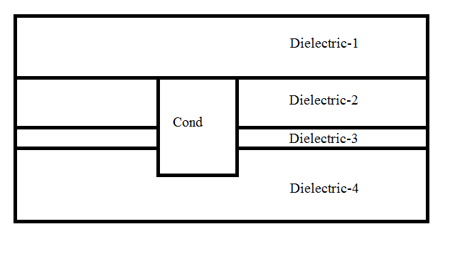
substrate stackup in ADS software

The easiest solution is to "stretch" one end of the via with the mouse, so that it goes through multiple dielectrics.
Another approach is to use "derived layers" to create clones of your via
qthelp://ads.2016.01/doc/usrguide/Adding_Derived_Layers.html
and map these new via layers separately.
The problem is that I can not make the width of the conductor bigger than the width the dielectris. For example if Conductor is 900nm wide, and Dielectric-2 is 700nm wide, I can not make Conducter's width bigger than or equal to 700nm. That is why In the next dielectric layer I have to map the same conductor to achieve a 900nm width. But this is not allowed by the ADS software. Any idea how I can do this?
You just need to split your bottom dielectric (dielectric4 in first post) into two pieces, so that you have a 200nm dielectric segment. Then, define the via to pass through dielectric2, dielectric3 and that new 200nm dielectric.
stackup substrate software 相关文章:
- Stackup agreement between SW Tools and PCB Fabricator
- Antenna design with 'Air Substrate'
- Ceramic or High K PTFE Substrate
- How to mount RF substrate into a Al housing for making an RF module
- best MS substrate to use in a wireless energy harvesting (rectenna)
- Substrate to substrate interconnect between two CPW substrates
