what's the best way to hook up VNA to PCB?
The down-side is that the calibration is slightly off from the actual measuring location due to the soldered-on connector.
I'm measuring around 915MHz.
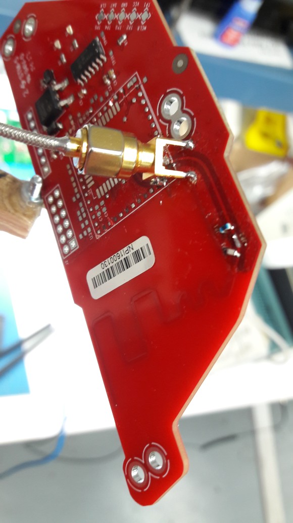
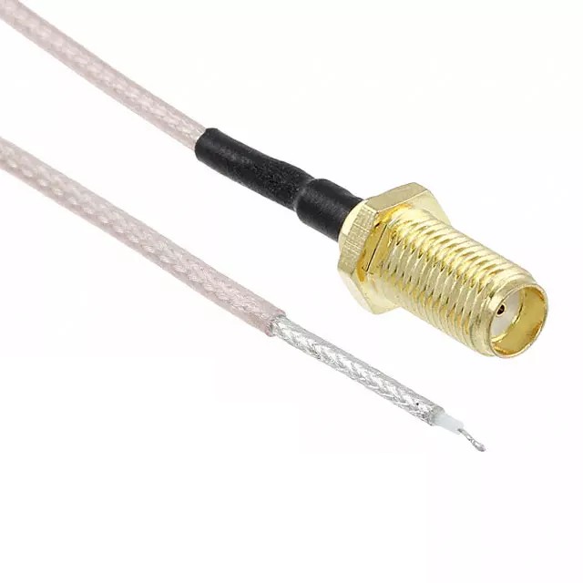
Someone told me that it would be smarter to get a coax cable such as shown below, and solder it directly to the board. The downside is I can't use the calibration kit, so I would have to use a good old 50 Ohm resistor, and simple open/short to calibrate.
Which method would yield better results? If it's the second one, any special considerations for the 50 Ohm resistor (probably high accuracy)?
At 915 MHz, the connector essentially has no effect. Go with the SMA.
Suggest to review previous threads, e.g.
https://www.edaboard.com/showthread.php?t=227177
https://www.edaboard.com/showthread.php?t=217756
Besides connector issues, it's unlikely to get reasonable results without suppressing cable effect. At least use some ferrite tubes.
My personal favorite for sub-GHz is U-FL connector cable with self made OSL calibration kit.
Suggest to use the pigtail.
http://rflabsinc.com/Products/Cable_...5/0915/55.html
Thank you guys very much and I also read the info that was linked to. That is exactly what my thought was too, that a pigtail with the simple method of short/open/load calibration beats adding in a connector and using a professional calibration kit.
I didn't even know about the ferrite (still learning obviously), looks like it will reduce the effect of the shield of the cable changing the characteristic of the ground plane on the PCB. I will give that a try!
I presume you are measuring the impedance of a mobile antenna, not using any ground plane extensions or external connections in operation. Then the VNA cable common mode impedance should be eliminated by ferrite beads/tubes.
A simple check goes like this, touch the cable in the middle, with sufficient ferrite isolation between antenna board and your hand, there should be no impact on the S11 plot.
Yes, this is an important effect that I have seen with such PCB antennas. The ferrite must be included for reliable results!
"ferrite isolation between antenna board and hand?"
i am not sure what that means at all. If you have to hold the antenna board in your hand, how about attaching the antenna board to a 2 foot long wood dowel, and holding the end of the dowel?
I personally would use the flexible pigtailed cable. I would put ferrite isolation beads along that cable (at least two of them) so the cable ground plane does not become a 2nd re-radiating antenna.
For calibration, i would do a response calibration, while temporarily shorting out the center conductor of the flexible line to the antenna ground plane with a blob of solder. Then set the reference plane of the network analyzer to show a short circuit, unsolder the blob, and read the impedance of the antenna off of the smith chart display.
"ferrite isolation between antenna board and hand?"
Sorry for being unclear. I described how to check if you fitted enough ferrite beads. Completely agree with your suggestions.
yes the hardest thing to do when trying to measure a tiny antenna....is to separate the effect of the flexible cable, and even the metal enclosure of the VNA.