[Moved]: analog filter input/output termination match
I thought I just need to guarantee its AC response satisfy my requirement (BW and notch in elliptic filter). I don't understand why I must guarantee impedance matching at input and output, but from electronic design handbook, it mentioned that input/output should be matched but it didn't tell me why I should do that.
Can anyone tell me why should I have input/output impedance matching? I think this is not a transmission line as the circuit size is much less than 1/4 of the working frequency wavelength, so why do I bother to have impedance matching? For maximum power transfer?
Can anyone give me some insight?
Source and load impedance are part of the transfer function. The printed filter parameters are only valid with the given termination. Use a circuit simulator and try.
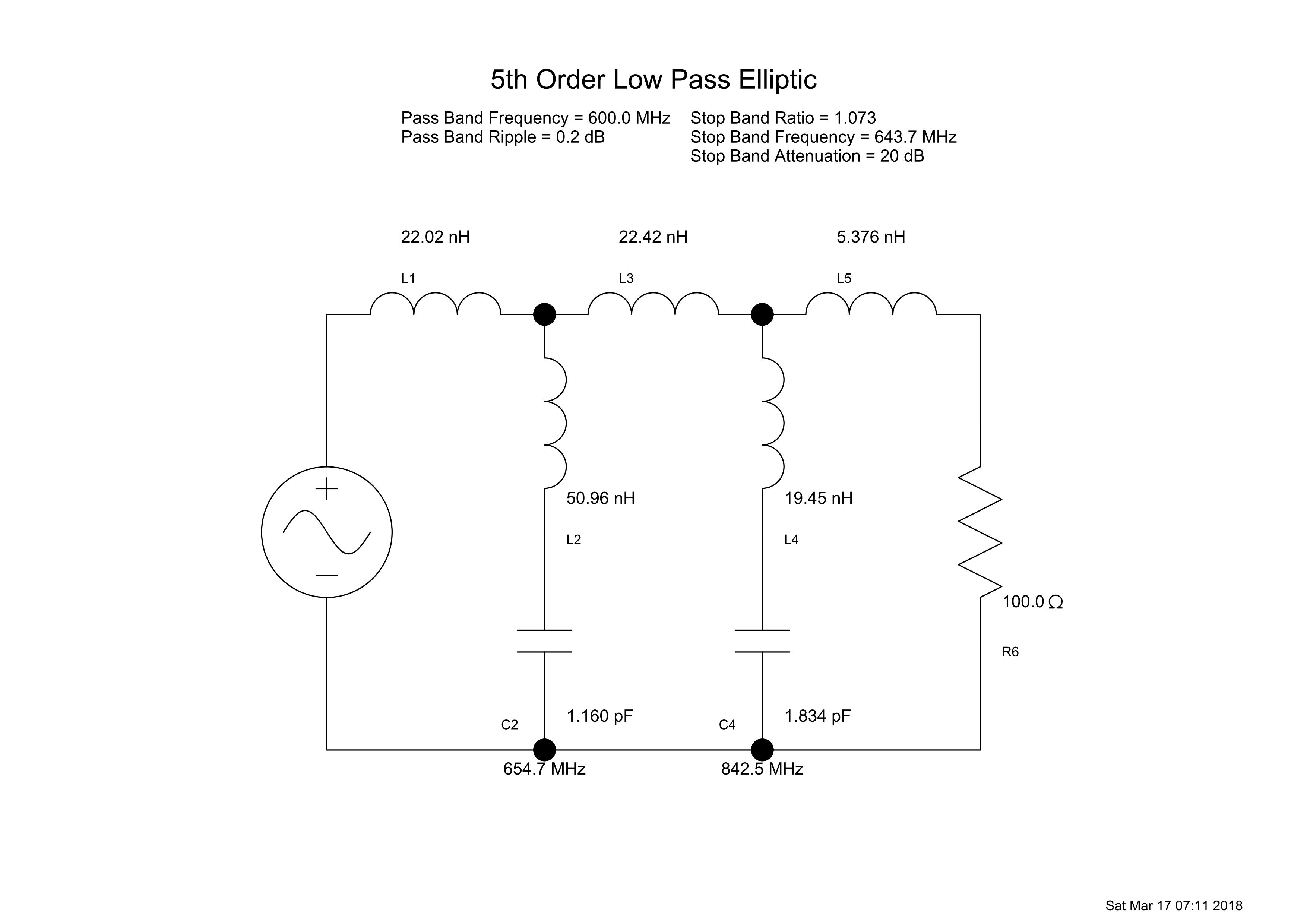
You can also evaluate the effect of termination variations in Filter Solution with "freeze" + varying circuit elements. Or the other way around, change the termination and watch how the filter elements are varied.
If you don't match impedance you get reflections, loss of signal integrity and all sorts of other horrible things.
How to understand the reflection or loss of signal integrity if there is no transmission line? For example, the time for the signal reflected is so short that you can just view the circuit as lumped element with Voltage source, source resistor and load impedance, total three components.
Can I have the question more specific?
I have the below circuit simulated in Cadence ADE
By varying the source impedance from 50 Ohm, 120 Ohm to 1K Ohm, I obtained 3 difference AC response as below. Can I use this circuit or not because I don't have source impedance matching?
I am really frustrated because I asked two engineers on my site but they reply me the same answer regarding termination and I need to match termination. What's wrong with the circuit that I miss consideration.
Any matching cannot be said on this filter because the load is not obvious.The filters are generally designed with source and load impedances ( in fact resistances ) and the filter coefficients are found as a function of many parameters including source and load impedances/resistances.So, you should try to find a appropriate filter which satisfy your requirements.
Note that, design of a filter for complex load and/or complex source impedance is more difficult because it needs to match doubly/singly terminated filter synthesize procedure that is pretty complex.
I don't exactly understand your problem. The filter can be designed for any termination, including complex ones. The only requirement is that either source or load have a sufficient real part. But the termination must be constant, otherwise the filter characteristic changes as well.
I presume you noticed that Filter Solution makes it easy for you to design filters with arbitrary termination like you have in post #5.
I can understand the part of source/load impedance contribute to the overall transfer function. Do you have any book to recommend?
This frequency domain transfer function satisfy my requirement but what I think is that it seems there are some other requirements that I miss to consider, impedance matching is one of them. Also, isn't that quite common to have capacitor load?
I am sorry for so much questions, I just cannot figure out what is going wrong? I want to use this circuit structure and further develop it based on what I observe in simulation, but I don't understand why the termination matching is a concern here? is there some simulation that I forget to run and check the performance?
The OP asks why does he need to match a load in the first place, what is the reason behind load matching, not how to match one. It was already answered in post #3. He also answered himself in post #1, "for maximum power transfer".
If the load is not matched, the source needs to provide reactive power besides the active power, increasing then the total RMS currents in the circuit, hence losses. Matching the load gets rid to the reactive power and hence less stress is taken from the supply and less stress (in terms of RMS currents) is on the circuit elements.
Matched load means only active power is supplied.
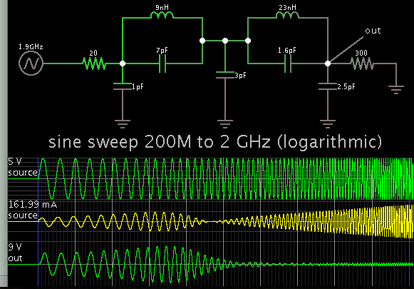
Your graphs show that greater source resistance results in greater attenuation of Ampere level. Notice that changing input resistance does not change the LC resonant frequency. The theoretical formula for resonant frequency is based on L & C.
When source impedance is very low, it may result in undesired behavior. This simulation shows what happens with your filter in post #1, after changing the input R to a 20 ohm resistor. Notice greater Ampere level being taken from the source as frequency increases above 1 GHz, diverted to ground through the series capacitors. The loss can mount up to several watts.
Also notice the output impedance is now a higher resistance. At a certain spot on the curve it results in gain in output amplitude. This is created by the LC combinations at resonant frequencies (unpredictably through certain combinations of paths). A 1k load results in 18V amplitude (from a 5V source). This is merely a simulation, naturally, although it illustrates concepts of behavior which might come into play.

You need a "single terminated filter"! Please note: If you have a voltage source, the filter must start with a series element.
In case of a current source, the first element mus be a parallel element.

Attention: Please read what the difference is between doubly terminated and singly terminated! You must understand what you are doing.
Read the user manual of FS, or go to the library:
Gabor C. Temes, Jack W. LaPatra: "Introduction to circuit synthesis and design"
Gábor C. Temes, Sanjit Kumar Mitra: "Modern filter theory and design"
I didn't yet hear a clear statement about source and load impedance of the application of interest. Post #5 e.g. suggests real source and reactive load impedance.
Some contributions refer to impedance matching in the context of maximum power transfer. As far as I understand, it's not an application requirement here. A specific filter input impedance as transmission line termination can be required in some cases, but it's only achievable in the filter pass band. Out of band signals will be mostly reflected.
Agreed. First of all, the requirements and the application must be clear. This is a typical case. Someone has a program and doesn't know what to do with it.
Can be solved with a diplexer, but this is a very elaborate design.
I am designing a filter with a notch at 800MHz to block interference while keep the BW of the filter >=400MHz, it's a baseband analog signal. The input is a source follower with a 100 ohm res in series (1/gm=20). The output of the filter is connected to a source follower, which I assume is a cap load. The AC coupling has a 5pF cap in series as shown in the post #5 above.
What I intended to do with this structure is to change the voltage source with small Rs (source follower) into a current source with high impedance Rds, and change the load from cap load (source follower gate) to a resistor load around 1K ohm.
I have ran AC analysis with the modified structure, it seems AC response is OK. I have the BW and also the notch at 800MHz. But the other engineers told me that I should consider the termination, which I really don't understand what's going wrong. A lot of replies here make great sense.
The first configuration seems preferable to me, the filter can be perfectly designed for the given source and load impedance (100 or 120 ohm source, small capacitive load). But the second is feasible as well. The load capacitance should be still put in the calculation.
You can check which impedance combination gives more comfortable filter component values.
As for your colleges suggestion, can it be that they aren't aware of the option to design filters for different source and load impedance, including complex termination?
If you have a AC coupling with 5pF it's hard to build a "true" low pass filter (cut off frequency). I think you can go with a bandpass filter? Give us some information about the passband: lower cut-off frequency and matching (Return Loss, VSWR?).
A source follower as a load might be hard to match to. I'd recommend adding a dummy load on the filter output in the range of 100-1000ohms. In theory the achievable insertion loss will increase, but it will make it far easier to get the desired frequency response.
Normally before starting such a design you should be equipped with specific measurements of the input and output impedance across the bandwidth of interest. Describing the load as "a source follower" doesn't really help.
Hi, Niki:
bandpass filter is correct or more specifically from my perspective, it's a 5th order elliptic low pass filter with AC coupling load.
I just realized the 10K ohm resistor's role in the loading stage, so I added it in my figure below. Hence the low frequency cut off is 3Mhz.
About matching, is that 10K ohm help explain the matching? Should I match the input to 100ohm and output to 10K ohm?
About Return loss and VSWR, how can I simulate it? Can s-parameter simulation (S11 in smith chart plot) give return loss? I will check if sp analysis can give me VSWR as well.
Hi, Mtwieg:
I just realized the role of a 10k Ohm res to AC ground at the loading stage (see figure, the original structure is fully differential, I thought the 10K ohm is part of a DC bias point feedback loop). I think that is what you mean the loading. It also defines the lower side cut off frequency.
Maybe something is not mentioned. The original designer of this circuit is not with this group any more, so I have to guess what they are doing. I find out the impedance of the LC network by Cadence sp analysis (circuit on the right starting from the 350fF capacitor).
It shows that when source impedance is 74 Ohm, the load can be 74 ohm purely resistive at 489MHz. At the original source resistor condition, which is 116.5 Ohm by connecting 100 Ohm in series with source follower 1/gm=1/60.5m=16.5 Ohm, the load impedance is as close as 107+j*26 at 52Mhz. At this frequency, it has minimum -18dB attenuation in S11. At Rs=74 Ohm, the S11 shows better matching and hence lower attenuation (-41.7dB at 489MHz) as well. Here is one more questions I have, the match only happens at one frequency while my band of interest is from around 3MHz to 403MHz. How will this matching help to reduce improve power factor or impedance matching?
