RF Power Amplifier design
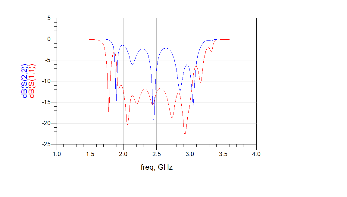
Note: BW= 2 to 3 GHz
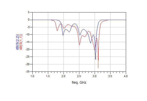
A 10 dB return loss will give you 90% through power. Which is a typical spec criteria.
In your case, you will lose a lot of power from 2- 2.4 GHz.
S-parameters are not much considered in PA design.
Instead, Load-Pull,Optimum Load Impedance,Optimum Source Impedance are more considered.
Ofcourse, load pull analysis is an important step without which you don't know what impedance - power to match, but the small signal response is necessary as well. Initial design methodology always goes through small signal response (small signal stability analysis). This is purely a standard academic design process point of view. When the designed PA shows instabilities, you will have to backtrack. Not everyone has the resource to do a large signal stability analysis, e.g NDF, Nyquist plot analysis or even a HB analysis.
Tq for information
In the attachment, after optimisation
Thank you
Are there any way to reduced it?
This is just fine. But more than this, you need to look at how close you are to optimum load impedance? Do you have load pull data at these frequencies?
I'm assuming you are using some sort of GAN on si power tranisistor.
Nope I do not have load pull data
Hi
In designing RF Power Amplifier, how we can know that BW is achievable?
Note, I am doing design using ADS.
TQ
Hi
In designing RF power Amplifier, What does affect S11 & S22 Input and output return loss?
I design the input and the output match network using the optimal input and output impedance from loadpull, but after that S-parameters especially S11 and S22 is always larger than -10dB. And how can I deal with it ?
It's normal because Optimum Load and Source Impedances are not Complex Conjugate of s-parameters.It's a problem of compromise.You will select a optimum point that will give between a better Reflection Loss(es) or Maximum Power.
In fact, the compromising points are more than this. Better Gain or Better Efficiency,Better Power or Better Efficiency so on..Therefore designing seriously a Power Amplifier is a really tough task.
But matching conjugate of S11 to Source Impedance is practically will eliminate some constraints.At least S11 will be closer to ideal case.Focus on Load side, it's the key zone to work on..
As you know well, these s-parameters are not independent ( I wish them so) due to S12 so while you're playing around one the other starts to move or vice versa.
Matching S11 to the Source then fix it there will accelerate the design steps.
but how can I get the optimal source impedance for a better s11 ? use source pull in ADS ?