Routing a RF signal through PCB metal plane by via-hole
In order to solve some mechanical issues, we want to route the microstrips of a RF board through internal metal planes.
We know that as general rule all RF signals must be routed on top metal plane with a underlying ground plane. Therefore, we do not know the consequence of a possibile routing through a internal metal plane, letting route the RF signal through a via-hole.
Do you have any advices about this topic?
Many thanks.
Regards,
Antonio
What is the operating frequency ? If it's really high, it will create a discontinuity and consequently a strong reflection at that point.
I also depends on the substrate thickness and via's diameter,plating thickness,plating materiel and quality.There will absolutely be a reflection in any event.
The board is a receiver. The frequency before the downconversion is about 2 GHz, after about 400 MHz.
yes that is a possibility. Run a stripline 50 ohm line in the middle of the board. You will need a TON of via holes on either side of the line to contain the energy. And make the run as short as possible, as it will be lossy.
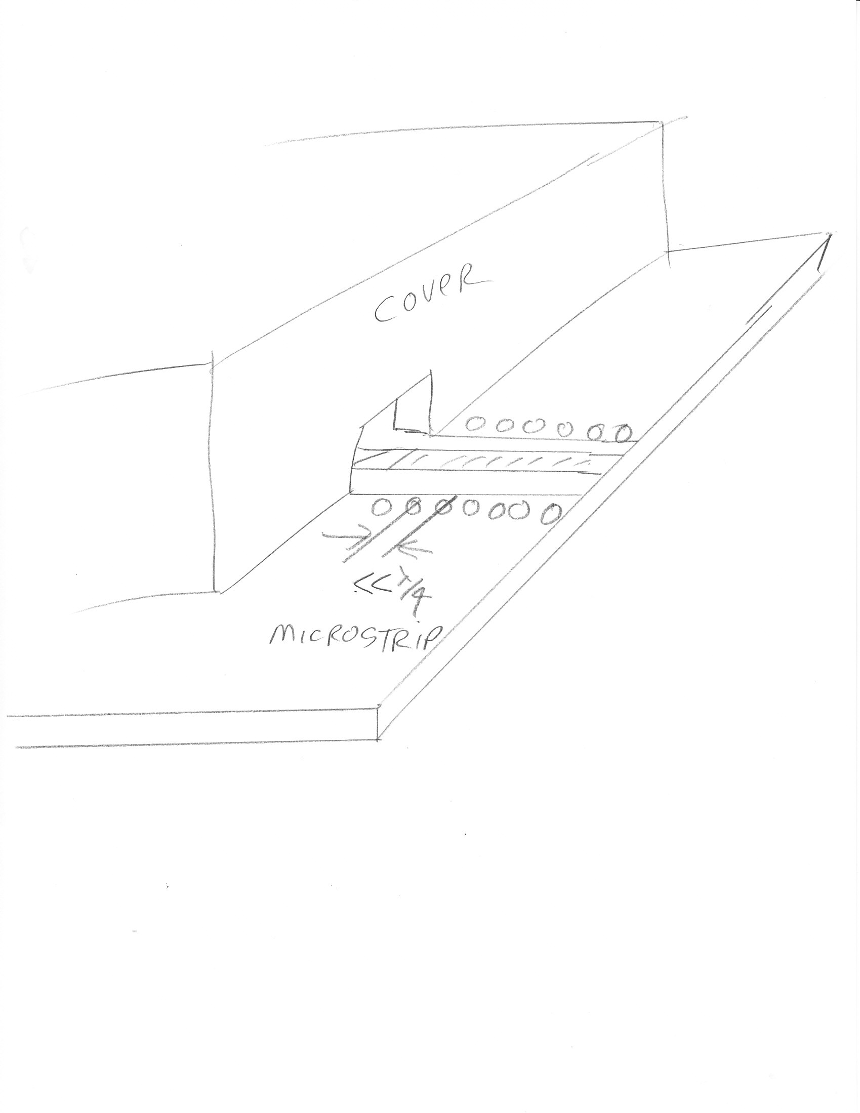
What i do often is just put a rectangular notch in the metal cover, and pass regular microstrip thru it. Since the notch is very small, RF does not leak out much.
It is not very clear the meaning of "TON" word. Are you talking about "via fence"?
What is a rectangular notch? I did not understand what you have told me.

something like this
