Guidelines to design a custom RF T-pad attenuator
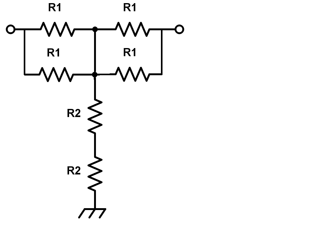
We are using some custom T-pad attenuators to control the signal level of a RF receiver. We have selected some 0402 SMD resistors and designed a topology where there are two pair of two parallel resistors and one pair of two series resistors (see the attachment).
We foresee to use this topology at 400 MHz and 2 GHz, therefore we would like to understand how to create a optimum layout on PCB in order to minimize the leakage between input and output, and reduce other parasitic effects.
Are there guidelines we can follow for an optimum pcb design?
Many thanks in advance.
Regards,
Antonio
If you connect the pads as short as possible or back-to-back, there shouldn't be any problem.
Choose the resistors high quality film type and stable ones.
Controlled impedance PCB design requires experience on tolerances of effective relative dielectric constant and loss tangent for the choice of MANY different types of epoxy,fiberglass,polyamide, ceramic, teflon, etc materials. I suggest you start with Saturn PCB design tool if you dont have anything.
Then enter the frequency of interest, research suppliers with best material of choice ( low loss , high f , stable, reasonable cost) then consider tolerances are cheap for 0.1% R's but expensive for <10% on dielectric so Impedance testing costs money or find good supplier who can advise you on options.
You haven't mentioned what attenuation you need. If attenuation results in high resistance values, parallel capacitance matters, so you might want to cut out backside ground underneath the resistor. For low resistance values, small series inductance = short layout path is required.
When selecting resistors for 24GHz PCB, I learned that different cut styles in laser trimming also affect performance, see
https://www.vishay.com/docs/60107/freqresp.pdf
I am talking about 2 dB, 3 dB and 4 dB attenuators. The biggest value of chosen resistors is 180 ohm.
May you explain me a little better the issue about cutting out backside ground underneath the resistor?
Many thanks.
Antonio
Hi Antonio,
cutting the backside ground is just to reduce the parasitic shunt capacitance. For your values, I don't think you will have an issue at 2GHz.
Best regards
Volker
i am curious why you would not just purchase a commercially available T pad? Cost issues?
Cost issues and to customize the attenuation value because we do not know exactly the total gain of receiver.
custom design Guidelines 相关文章: