[ADS] The Accuracy of DC simulation in ADS
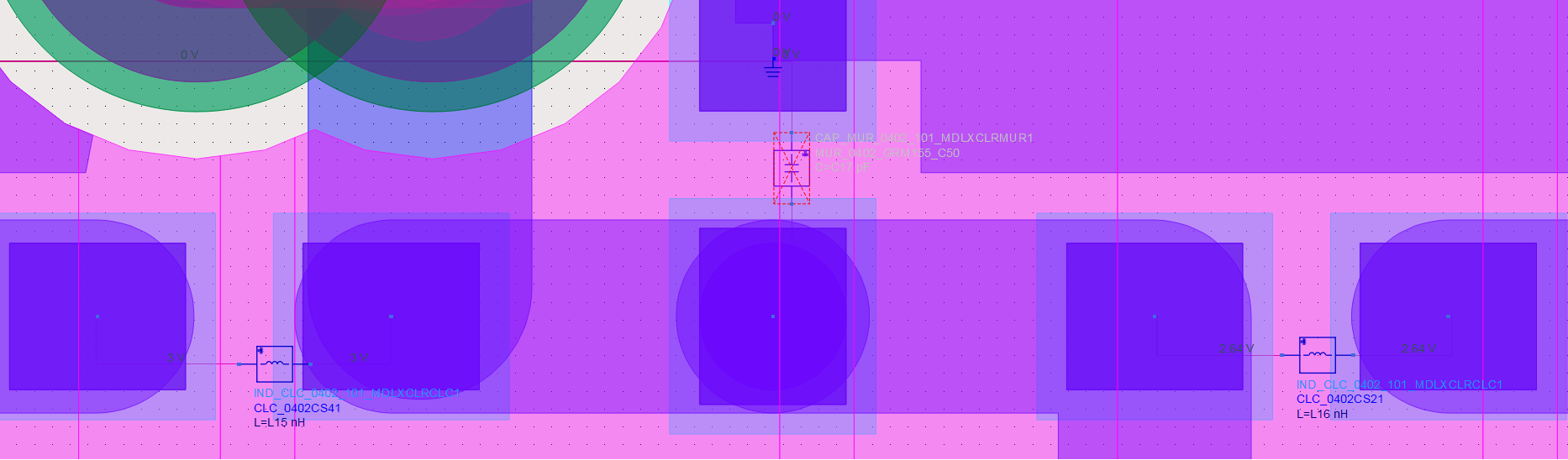
Please refer to the attachment. The DC drops from 3V to 2.64V after going through a short transmission line which it doesn't make sense. From my experience, its wrong and in the real world, it will be almost no voltage drop. my questions are;
1) why DC simulation is not correlating with the real world measurement? It is the limitation of the DC simulation controller?
2) How to make the DC simulation correlate with measurement. do I need to increase the mesh count?
any other valuable input in the subject matter is appreciated.
I already explained the effect in your previous thread: if you define ports with explicit ground references, then only the voltages between each port (+) and (-) is known. These S-params don't have information on the voltage between different (+) or different (-) pins.
This is simple physics (definition of S-parameters) and not related to ADS. From the S-params, you get the voltage at each port measured between port (+) and (-). Your problem is that all your ports have different grounds, and you don't have information on the voltage between port 1 (-) and port 2 (-). Or between port 1 (+) and port 2 (+). Each voltage is only know with reference to the local (!) ground of this port.
If you want your model to pass external voltages, or know the impedance between pins that belong to different ports, you need to ungroup the pins, so that signal layer and ground layer pins have separate ports. All these ports then have the same (!) ground reference (an abstract "ground at infinity") and become physcal again after making proper connections at schematic level.
Summary: the issue is not related to accuracy, it is related to different ground references. To test this, start with a very simple testcase with just 2 lines.
hi volker, thanks for the reply. i recall our earlier discussions where you said grouping pins (+ve pin and -ve pin) to form a port is needed in my case because i don't have an infinite ground plane at the bottom.
in order to ungroup pins, i need to select bottom as infinte ground plane? i can do that because the bottom is dedicated to ground and also DC only. for your information, im using coplanar and not microstrip.
thanks.
Yes, but this limits what you can probe from the resulting data. It is also ok to simulate your device with pins vs. global ground and make the proper connection at schematic level.
I think you can also go without infinite ground plane, then Momentum uses an abstract "ground at infinity" for reference. I don't know what warnings you might see then. Try with a simple test case first, just two lines using your stackup, to test DC connectivity and see if warnings are shown.
Hi Volker,
I have deleted all the ports with both -ve and +ve pins and added all the layout pins which include ground (-ve) and other pins (+ve) as a separate ports. EM simulation is going on. I will share the outcoming.
--- WARNING -------------------------------------------------------------------
Port 1 does not have an explicit reference pin,
S-parameters may become unphysical at higher frequencies.
again the same error as before appearing for every ports (all 150 ports) . this is the reason why we decided to reference each +ve pin with adjacent -ve pin before.
what do I do now? do I select the bottom layer as infinite ground in the layer stack up? if I need to do this will the simulation be accurate or am I doing something wrong?
in order to make bottom layer as an infinite ground plane, I just need to select that layer and make it a slot plane instead of the strip right? actually, the bottom is just DC and ground. I can feed the DC at the TOP also without any problem.
please send your thoughts.
Yes, ignore that. Results become physical at schematic level when you connect things.
Simulation is just completed but I still the DC problem. The layout simulation is accomplished by making each pin as individual ports but when I do DC annotation, the ground pins are still shows negative voltages! due to this, I placed the ground symbol in every ground port.
the DC voltage drop issue which i pointed out before is still happening too! so our method basically didn't work!
I don't know what you did, but the method that I described works fine.
Workspace is attached. For this type of fundamental methodology questions, it is best to try it with a simple testcase first.
localground_wrk.zip
I found an article on your website too. i revisit my methodology again.
Volker,
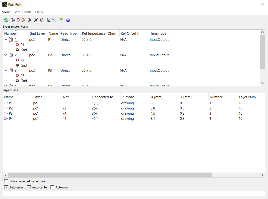
I have modified the GND of the Ports from Implicit to pc2 in your testcase.( You defined the GND pins of the ports with extra ports that are connected to local GND )
What will be trouble in this case ? I didn't see any warning or error during simulation and ADS accept as is.

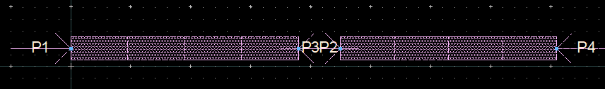
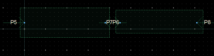
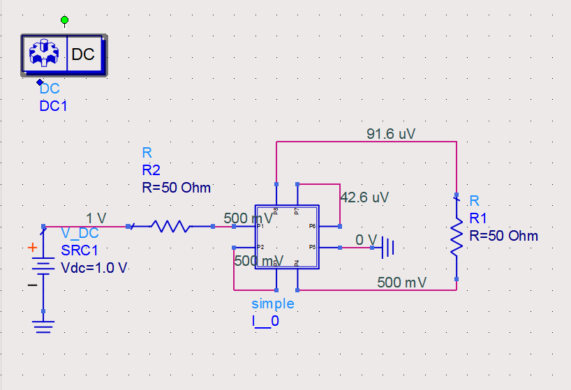
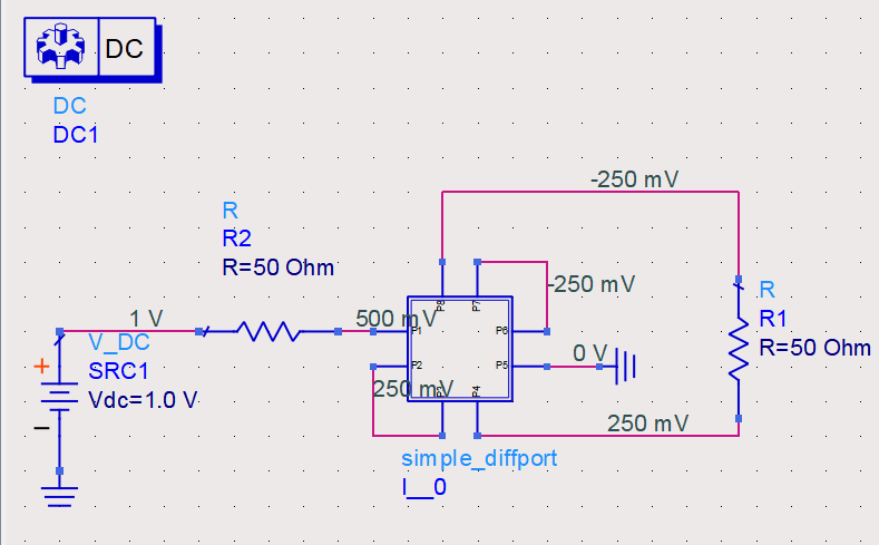
You mean like this, with the pc2 pins as local ground reference?
This is valid for the (exact) mode in simulation, i.e. all these port voltages & currents, measured between each port (+) and (-) terminal. However, with that reduction from 8 ports (common ground reference at infinity) to 4-port (different local grounds for each port), any extra information on voltage between other pins is lost. We then have only voltage & current at the ports: p1 to p5, p2 to p5, p3 to p7 and p4 to p8. Other connectivity (e.g. pin 5 to pin 6) is no longer available in the 4-port S-parameter result. The 4-port results do NOT tell us that there is a metal path from pin 1 to pin2, or from from 5 to pin 6. Reason as explained above.
Results: Even with port 1 reference connected to schematic ground, ADS doesn't know that the output resistor has one terminal connected to ground, through the cascaded metal strips. Instead, ADS assumes a symmetric voltage at that port. This is not an ADS issue, it is missing information when reducing the 8 pins to 4 ports with local grounds.
Dear BigBoss,
The article below from Dr. Volker will give better clarity.
http://muehlhaus.com/support/ads-app...r-differential
Dear Dr. Volker,
i figure out what went wrong in my simulation. my simulation setting and yours are exactly the same. After simulation, i got an error as below;
The instance `X1' has 148 pins, but the view `XXX:schematic' has 0 pins.
Due to this I clicked "choose view for my simulation" and select emModel! That's where the mistake is! when I select layout instead of emModel, the simulation DC annotation results came as expected.
i also figured out that i need not connect ground symbol to any ground port in the layout lookalike component and the voltage at the gound port is always 0V. thank you.
by the way, i generated new emModel by clicking EM --> Component --> Create Em Model and Symbol right after the simulation. but i dont understand why this problem happened!
I don't understand what you did.
The normal procedure is to create emSetup, emModel and Symbol. There should be no schematic view in this cell, then emModel is used for simulation and everything works fine.
1) i got this error;
The instance `X1' has 148 pins, but the view `XXX:schematic' has 0 pins.
2) I selected layout lookalike component and clicked "choose view for my simulation" and selected emModel!
3) I simulated the schematic. I got non-zero values for all the ground ports for DC annotation.
4) I selected layout lookalike component and clicked "choose view for my simulation" and selected Layout.
5) I simulated the schematic. The DC annotation results seems good with 0V for all the ground ports. i didnt even connect the ground symbol!
yes. in my case, i also did that.
there is schematic in my cell view! this is the celli did EM simulation too. please look at the picture below.
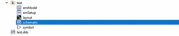
my question is how to avoid schematic in the cell?
This usually means that you haven't created an emModel. The default hierachy policy selects emModel if available.
That's usually the wrong choice. I really don't understand your workflow/methodology. But if it works, that's fine!
what you are saying is making sense. i don't deny that but i didn't make those mistakes. I click EM --> Component --> Create Em Model and Symbol right after the simulation without fail, everytime. my model settings are as below.
this is weird. I'm getting sensible results due to this.
I think my mistake is here. maybe I did mistake by saving schematic in the same name as the layout so schematic appeared inside layout cell.
Yes, that will cause trouble because Schematic view will then be used for this cell, instead of emModel view.
I have seen that mistake a few times, where the testbench was stored in the same cell as the Layout/emModel. Don't do this. Use separate cell for testbench.
Dear Dr. Volker,
i have verified in the simulation with emModel, Layout and symbol. even if i save the cell with different name, "Let the Hierarchy Policy determine which view to use" or choosing between emModel and symbol giving garbage results with DC annotation doesn't make sense.
only when i choose layout, i get sensible results.
results doesnt make sense means ground ports showing different voltages as compared to each other.
sensible means, when i connect one ground to ground symbol, the rest of the ground ports shows 0V. voltage drop is also sensible.
Ok, one final try. Maybe you are still using multi-pin ports.
There is a setting in each mModel how to handle the "undefined" portion of data, for paths that are not covered by the reduced S-parameters.
I can't comment what you should do. Check your results carefully.
please let me know how to access this menu. thanks.