Strange oscillations at the output of a MAR-1SM
I must clarify that this circuit captures the signal of an antenna located at about 15 mm.
Is there an alternative way to avoid the use of that trick to avoid spurious oscillations?
Thank you in advance!
What is the frequency of the spurious oscillating? It sounds your output signal is fed back to input port through the air. You may try to put the amplifier inside a shielding can.
Oscillations occur in many ways.
The most probable oscillation source the layout and GND connections of the device in this type of application..
The layout must be carefully designed and any emitter/source inductor shouldn't be there due to feedback effect.
If you post your layout, I can comment more concrete.
Thank you for your advice. I'll try it later.
The circuit is part of a mixer that detects shifting in that frequency caused by the alteration of the dielectric present in an electric field generated by two planes (as plates of a capacitor, one the emitting antenna and another the receiving one).
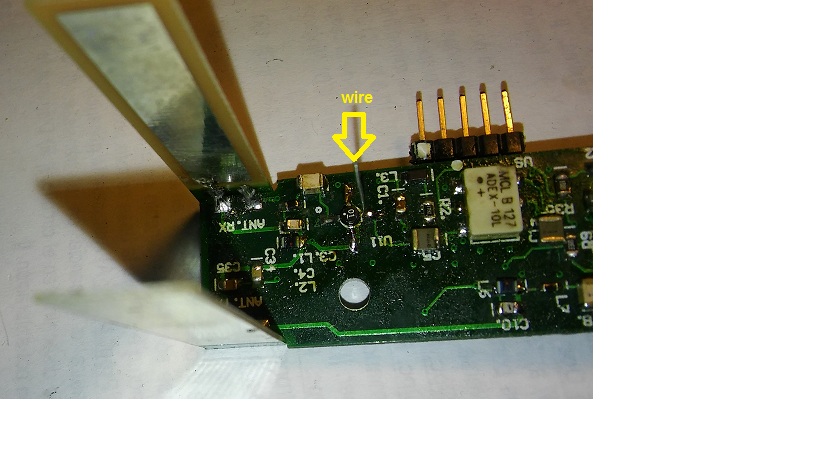
At the exit of this arrangement is the monolithic amplifier. If I extract that wire, I get high frequency oscillations at the low frequency filtered output of the mixer, although not continuous. If I put the wire, the circuit works correctly.
Unfortunately I can not leave the wire for constructive reasons.
What else can I do?
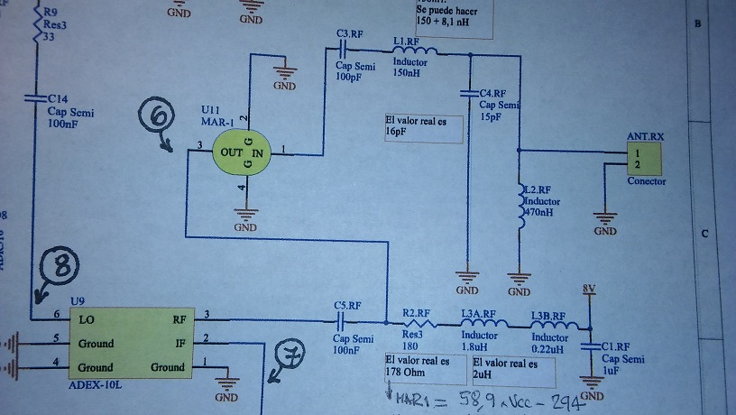
For the DC bias the circuit use an RF choke series with a resistor. The resistor value depends by the Vcc voltage.
At frequencies lower than 100MHz is recommended to remove the RF choke and let only the resistor in place. The gain will be a bit lower, but anyway at 40MHz the gain is too high.
Also try to increase the value of the bias resistor, even if you use the value recommended for the Vcc.
A picture,schematic,layout drawing tells more than hundreds words..


This is the diagram and real circuit.
Any additional suggestions?
Thanks, very much!
Clarification to the previous images: The wire is placed at the point marked 6.
The pcboards are of 4 layers, with planes of mass and vcc inside.
Oscillations are coming from Input side.Since the Input Impedance is matched to 50 Ohm why you have used a extra matching circuit ? Is antenna impedance different than 50 Ohm ?
GND Connections must be very tightly connected to GND layer ( underneath of the main layer ) and this connection should be ensured so no parasitic inductance shouldn't be presented.
Layout drawing will be helpful if it's possible to post here..
Thanks for your support.
Indeed, for constructive reasons.

This is the RF side. There's not much I can do now. Maybe the modification or added/removed of some passive component?
(Note the frequency is "only" 40 Mhz)
Also, I would be interested to understand why the circuit works by placing that wire there ...
Perhaps the shortest way would be to understand this and act accordingly from those deductions.
Replacing the wire by some passive component...?
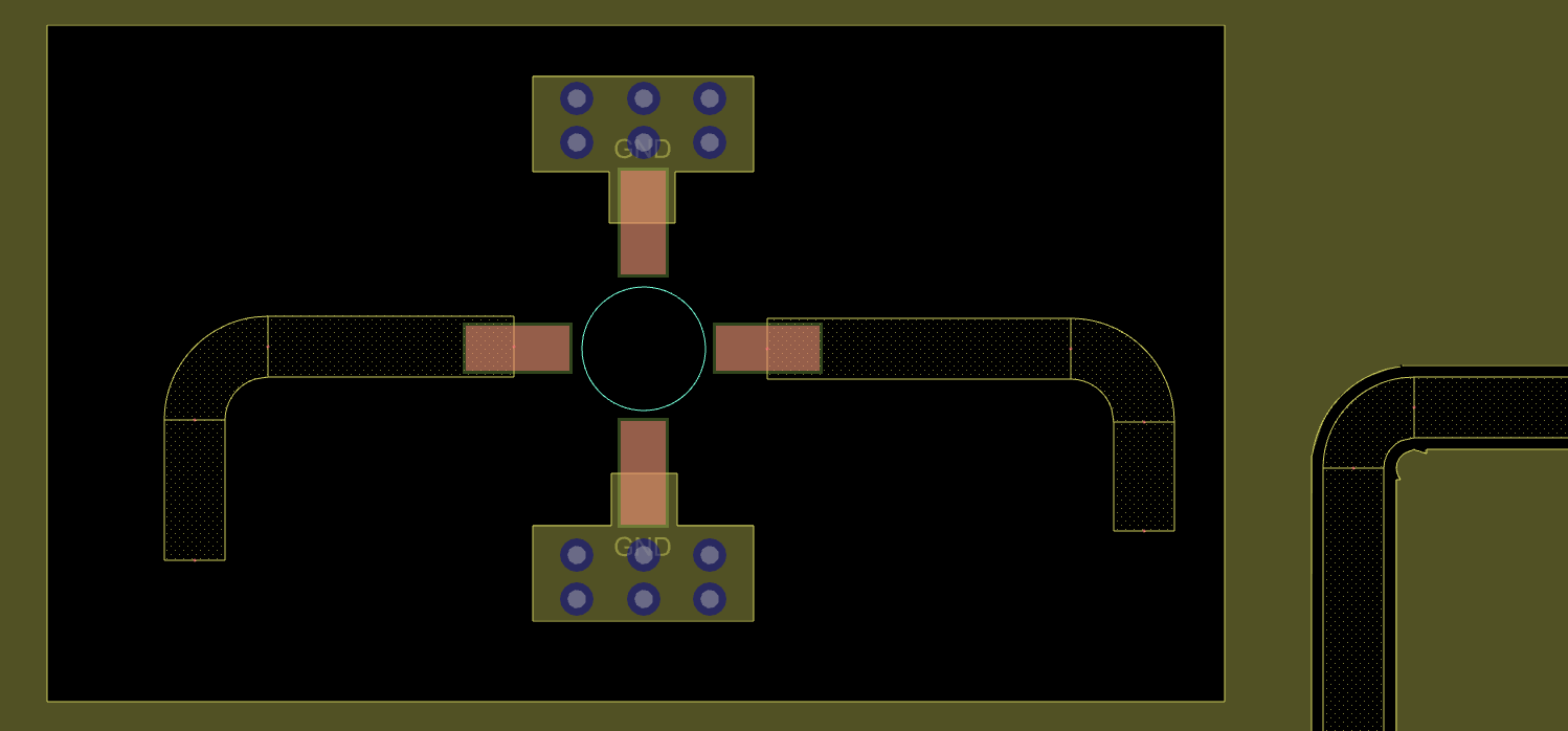
According to the layer 1 picture, this elementary principle of RF design isn't considered in the layout. MAR-1 should e.g. use separate vias near both ground pins. The rather large ground trace is likely to bring up oscillations. There are possibly ways to stop oscillations by killing the amplifier gain. To make the circuit work with full performance, the layout needs rework.
In case you have a continuous layer 2 ground plane, there may be chances to make experimental ground connections with a Dremel tool, removing the top prepreg near some ground pins and soldering down to the plane.
Thank you for your advice but, indeed, the manufacturer's suggested layout has been followed and below this layer the mass is connected to GND through some via (those small gray circles) that are not shown in the figure by clarity.
Your layout is too bad even your operating frequency 100 MHz.
I have explained many times here in many threads for the people that the Layout ( integrated,discrete,monolithic,any kind..) is the KEY of the RF Performance.Everybody should pay attention to RF layouts otherwise the circuit either oscillates or Gain drops very steep or the circuit does not work at all.
Typical Monolithic amplifiers layout should look like this..

You have to review your layout ( and other remarks ) accoding to my advices.
Absolutely agree with FvM and BigBoss, your layout looks really bad. You place one wire at the output may just disturb the feedback loop and destroy the positive feedback condition by chance. It can never be a solution for a serious product. Several general comments:
1. From the layout I can see that the 50 Ohm tracks have different track width at different places. The track width must be carefully calculated based on the PCB stack-up. If your component RF pins are significantly wider than the 50 Ohm tracks, you should cut-off the plane underneath the pins to reduce the parasite capacitance.
2. You should use RF capacitor/inductor with similar size of 50 Ohm tracks. It seems that you used EIA-0603 RF capacitor/inductor? EIA-0402 may fit better for your stack-up.
3. Place the GND via as close to the component GND pads as possible and use three GND vias for one pad if there is enough space;
4. Flood the top layer with GND plane. Keep the GND plane 3~5*H to the RF tracks, where H is height to the reference plane;
5. Use shielding can if there is space. At least you should leave footprint for shielding can(s) in case you have to use them;
6. Add a Pi impedance matching network for both RF input/output port in case needed. Only mount the through component with 0 Ohm resistor. Put one pad of the shunt components on the main RF track and default not mounting the shunt components. This has very little impact to the main RF track.
Okay, I thank you very much for your valuable advice.
I will follow you strictly on the next prototype but, I need this current one to work now and it does it perfectly with the wire at that position.
So I ask anyone who comes up with a solution to replace it to help me so I don't have to try "blind" as I don't have enough experience in this field.
I would be interested to understand why the circuit works by placing that wire there ...
Perhaps the shortest way would be to understand this and act accordingly from those deductions.
Replacing the wire by some passive component...?
Again, thank you very much!
At 40 MHz the vias in a MAR-1SM design are pretty much useless, if a good planar ground plane is used.
Remove the series choke (L3A+L3B) and use only the series resistor for the bias (change R2.RF to 330 ohm).
The wire antenna is coupling to the circuit to these series chokes, and make the MMIC to oscillate.
It may be me, but I can't relate the statement to the layer 1 artwork shown in post #10. I understand that the gray points are throughplated vias, but apparently not connected to the MAR-1 ground pins.
The wire probably provides negative feedback or defines the resonant circuit, don't know exactly. I presume you can achieve a similar effect by adding a small capacitor or resistor. It's just trial and error.
Use GND Plane Layer for all GND connections including the Antenna.
Also, an antenna cannot be connected through regular connector.Use a proper RF connector.
The layout is really inconvenient for RF..
Brilliant solution vfone!
Indeed, by removing inductance L3 and increasing the series R2.RF, the oscillations disappeared!
Obviously you are an expert on the subject and I especially appreciate your advice.
To the others, thank you very much also for your contributions. I'll take them into account in the future.
Many thanks to all!
