12-way resistive splitter layout
Any advice will be greatly appreciated.
Before selecting suitable components and deciding about the layout, you need to fix the specification.
impedance matching required for both directions or only for input side?
acceptable Sxx error
power rating
Low power (1W will be more then sufficient), just a resistive splitter. We already tested 2-way and 3-way that I designed myself (402 package resistors), and they perform as expected (well, minus obvious FR4 substrate related loses), and layout was straight forward as far as star configuration goes. 8-way was designed by chaining Susumu 0803 packaged 2-way resistive splitters which of course required some traces routing and using CPWG technique (I personally didn't detect any significant difference between Susumu "qualified" 10GHz components and a good quality 0402 resistors from Vishay or Kemet for 2GHz-6GHz band), but attempt to try to layout star splitter for 12-16 way split is definitely different from 2 or 3 way splitter - I can't just put 13 or 17 resistors "back-to-back" to form the star. So main question is not about power handling or S parameters, but rather how to layout "RF way" 13 or 17 resistors in a star configuration arrangement (for 12 and/or 16 way resistive splitter).
I never layouted such a (lossy) resistive divider, only cascaded 3dB Wilkinson for 1:8 divider.
Here, I would start from a 1:3 divider and then cascade 1:2 dividers. This way, you can easily create equal path length.
Do you need the "round" layout, or can you have all 12 outputs side by side?
Cascaded design is exactly what I did for 1:8 splitter (similar to shown by Volker), but as I noted above, it was not a start configuration, but cascaded one. This approach gives 6dB port-to-port isolation (resistive splitter rule said that port-to-port isolation equals to loss), which is probably ok in my case. A reason behind desire to use resistive splitter (even though it is not the best approach from loses stand point) is desirable gain flatness within channel width. I already tried a high quality multistage Wilkinson with very low noise LNA at the entry (actually 3-4 from different vendors), BUT, it looks like that Wilkinson does not maintain needed gain flatness within 20-80 MHz channel that leads to radio's inability to correctly demodulate and decode frames (dual band WiFi). I have a much better results with resistive splitter approach with LNA compensating loses. I've been thinking about "round" design style with star configuration, but as I noted, have a doubts about appropriate layout that calls for joining 13-17 resistors in one common point. I found a few vendors who sells 10-13 way resistive splitters - probably one can just buy it, pop-up the hood and take a look, but they are prohibitively expensive. I wonder if anybody already had this challenge in hand in a past, or has an access to commercial 8 - 16 resistive splitter that can be looked inside - no way that they were able to join 13-17 resistors in one common point - it should be some other layout "trick".
If you look at my cascaded approach, that has smaller junctions (only 3 or 4 resistors), so it is much easier to route in a star configuration. You can "merge" the series elements into a single resistor, and keep the layout advantage of cascading. Few resistors in the center, increasing number towards the outside where you have more room (larger diameter)
"Merging" resistors is an interesting idea - didn't think about it. l will certainly try this approach and will report results - shouldn't take a long time to implement the prototype. Thanks! Which resistors packaging would you recommend for 2GHz-6GHz range? I can try 0603 for layout prototype, and 0402 and/or 0201 for final design (0603 is more friendly for hand soldering).
I haven't used resistors in the RF path for a long time, so I am not sure what the present status is. Back then, at 24GHz we used resistors that were specifically designed for RF (dot trimming rather than slot trimming). That's what I recommned to check: be careful with laser trimming styles. This can introduce quite some inductance even in small packages.
https://www.vishay.com/docs/60107/freqresp.pdf
Thanks a lot Volker for the article reference - I remember seeing it a while ago (didn't save it though - now I will) and concluded that 0201 packaging should work fine at 6GHz. I will try to layout something next week as a first attempt.
Thanks to everyone as well for answers and advises.
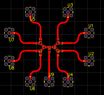
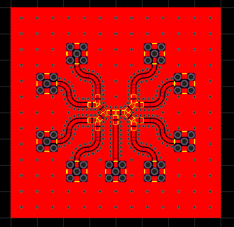
How this one looks like for 1:8 resistive splitter (with 0402 "merge" and MMCX connectors). Of course it will be CPWG with ground stitching in a final. Any opinion/advice?

Something like this - 0402 resistors, 0.6mm two layer PCB (FR4), 1oz copper, 0.65mm traces, 0.2mm gap for CPWG, MMCX connectors. Should it be ok for 2GHz - 6GHz, I guess?

I'm working in EM simulation, so I would simulate instead of estimating. The basic layout looks nice and symmetric. I assume that your line width calculation accounts for the extra capacitance (-> lower Zline) from the side grounds?
Unfortunately I do not have simulation soft at my disposal - it will be nice indeed to simulate it first and see what simulated results will be. The only thing that I can do is to create a PCB, assemble it and test it using my "cheap man" equipment, like RF Explorer Signal Generator and RF Explorer Spectrum Analyzer, and see how circuit reacts to signal in 2GHz - 6GHz range. I wish I would have an access to such a simulation package, but last time I checked it was prohibitively expensive. I use Saturn PCB Design Tool to calculate CPWG parameters such as substrate height, trace width and gap between trace and top ground layer. My current calculation gives me for 2-layer 0.6mm FR4 (0.51mm substrate height between top and bottom ground planes), 0.65mm trace (same as 0402 packaging pad width), and 0.2mm gap for CPWG impedance figure of 51 Ohm - good enough since I can't go below 0.2mm gap with my current PCB manufacturer, and going for 0.4mm FR4 would be a bad choice (it feels like paper in terms of rigidity). My understanding is that even FR4 in 0.6mm should be good for this frequency range (I tried to make traces as short as possible to avoid unnecessary losses at higher frequencies) - I recall an article comparing Rogers vs FR4 vs PCB thickness vs high frequency loses and do remember that FR4 in 0.4mm - 0.7mm range had an acceptable performance. Another thing that I think should work better vs my previous design is MMCX connector that eliminates necessity to create a separate approach for SMA landing pattern in order to maintain 50 Ohm impedance consistency and avoid impedance mismatch at SMA (I would need at least 1.1mm wide trace and 5-6mm length for the SMA pin to solder - edge mount SMA connector). MMCX connectors are rated to 6 GHz, so it should be good to go.
This is my plan of attack, so far.
Sounds fine. I asked because see some designers use microstrip calculator and then add side ground, which is obviously a bad idea.
If you upload your Gerber file, I might have time tomorrow to do a quick EM simulation. Just let me know the substrate - is it FR4 0.6mm then?
Correct, it is FR4, 0.6mm, 2-layer. I will generate gerbers later today, and will post Saturn PCB output showing CPWG calculation. Thanks a bunch for offering help! It will be really cool to see what simulator will show. I usually use EasyEda for PCB design and manufacturing - really cool and reliable service, I run about 150+ simple boards through them in a past, including some funky experimental PCB printed antennas (the only limitation(s) that that they have is max 6-layer and FR4 only, other then that the most reliable service and inexpensive as well, hands down).
Here is gerbers archive, Saturn PCB screenshot, and TXLine screenshot. PCB is FR4, 0.6mm, two layer, 1oz copper, traces 0.65mm, gap 0.2mm, MMCX connectors rated 6GHZ and over. Dying to see simulation results. Thanks a lot again!
R1, R2, R3, R6, R7, R8, R9, R12, R13, R14, R15 - 16.9 Ohm
R10, R11, R4, R5 - 33.2 Ohm


Ok, I created a simulation based on your Gerber file, but missed your silk screen and used my own port number (CCW direction). For the resistors, please have a look if you agree what values goes where.

Meshing in simulation is somewhat "quick and dirty", but results should be reasonable. I used ideal resistors, so we don't have the SMD body's shunt capacitance to ground included.

Volker - it's awsome! Thanks a LOT! To my humble opinion charts looks fantastic - I didn't expect them to be that good. It will be interesting to see these charts up-to 6GHz where looks like the most critical to the design data is. Also, I found a few "glitches" in few places in my previous 8 port grbers - is it possible to run your simulation one more time with updated gerbers and to 6GHz? And, you are right of course wrt resistors values (forgot an few places about "merging"). Since the goal was 12 port, I attached 12 port design as well - not sure if it will be ok to ask you to run simulation on this as well. In exchange for this favour I will send you a few PCBs once I'll get them from PCB house, if it's acceptable (not sure how much PCB house will charge for assembly in case there is an interest in assembled one). Looking at simulation charts I wonder what exactly contributes to S11 going up with frequency - is it FR4, connectors, resistors, or layout (second chart wrt to input to output ports is almost perfect since theoretical loss is 18.026 dB, and third one for port to port isolation looks in-line as well). So here it goes:
8-port:

Gerber_1-to-8-resistive-splitter_20190427001556.zip
12-port

Gerber_1-to-12-resistive-splitter_20190427001639.zip
-Don't use Thermal Relief for Connectors
-Pour-Off as much as possible around Inner Pin of the Connectors ( less parasitic capacitor )
-FR4 is pretty much lossy for beyond 1-2GHz, consider another Substrate ( Rogers, Taconic, ?)
-Use Horizontal SMD Connectors -if it's possible- because 90 Degree models have relatively more attenuation
Ooops ... I had done the EM simulation up to 6GHz, but by mistake used 5 GHz in the schematic testbench. Here is the result up to 6GHz - indeed that's most critical.

According to my simulation the line width isn't correct, this is what I get for the path from input port to the first resistor:

I might have some time early next week, but not sure because I'm busy with simulations for a client. Attached is my ADS 2017 workspace, in case someone else likes to double check.
resistive_splitter_wrk.zip
