power amplifier design input impedance
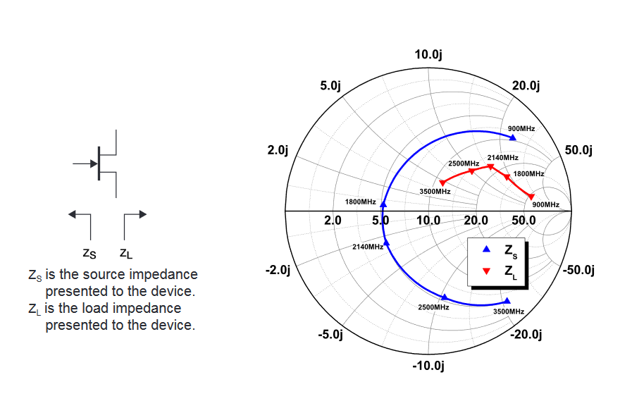
i want to design a power driver at 900 MHz. For this application i chose NPTB00004 transistor from maccom. In the datasheet they provide optimum load impedance and optimum source impedance for maximum power.
Attachment 151516
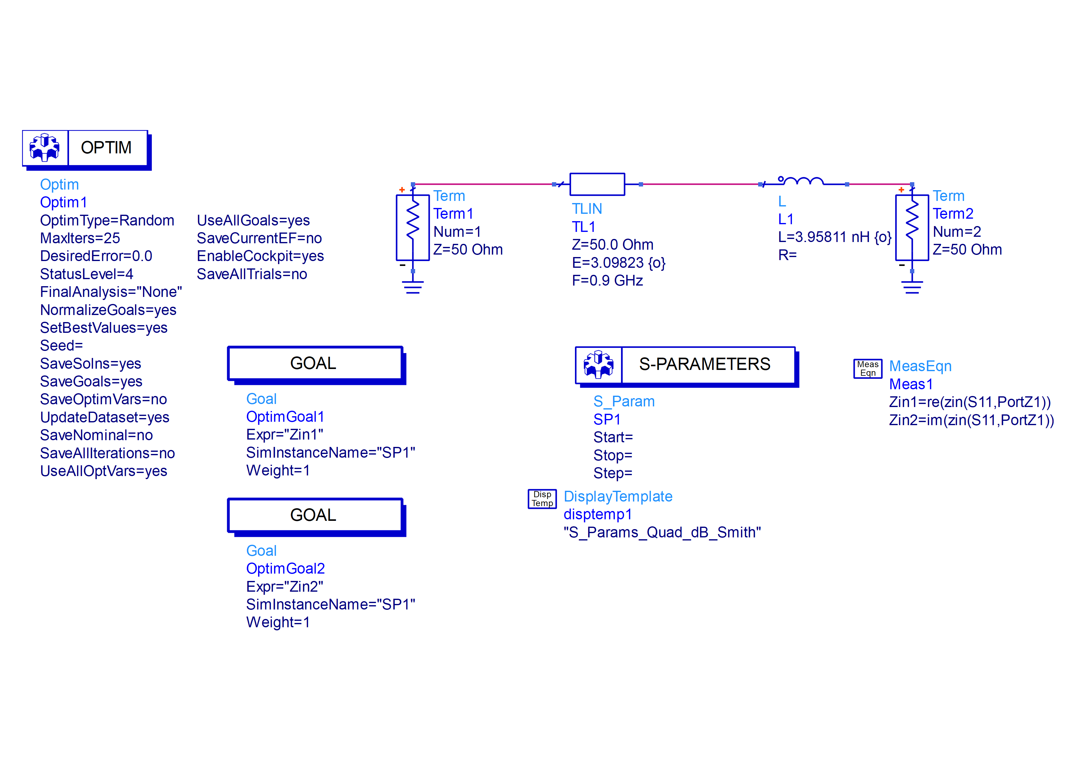
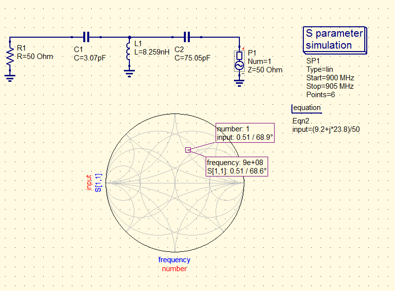
I designed a matching circuit for input and output as per the datasheet value for 900 MHz
Attachment 151517
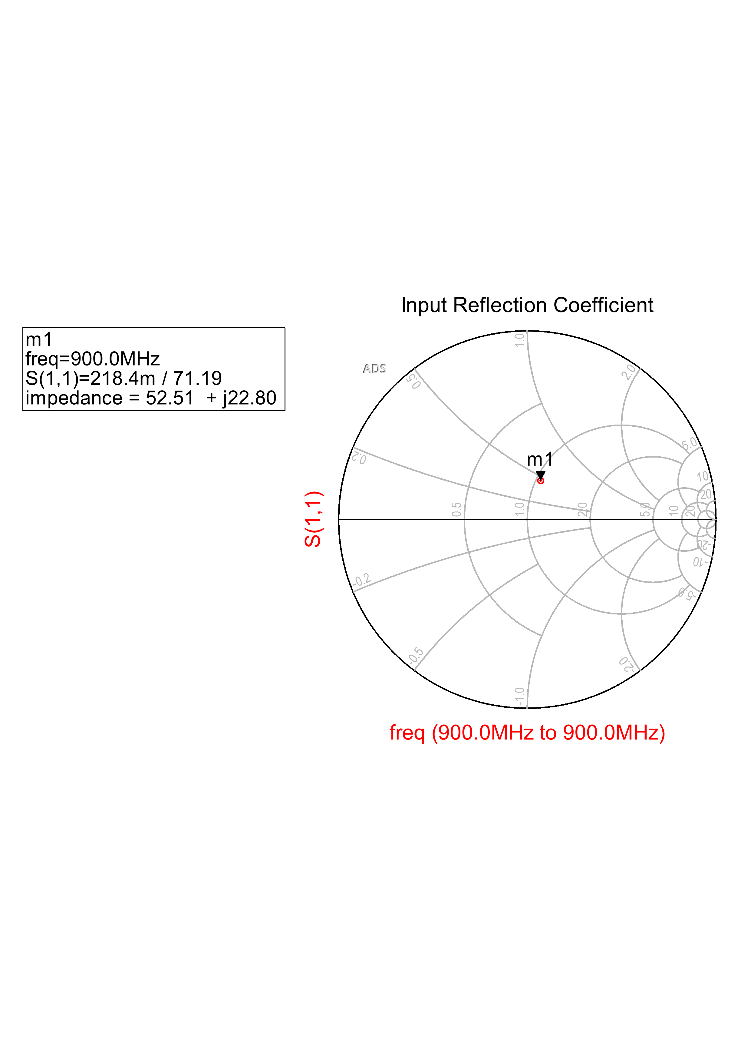
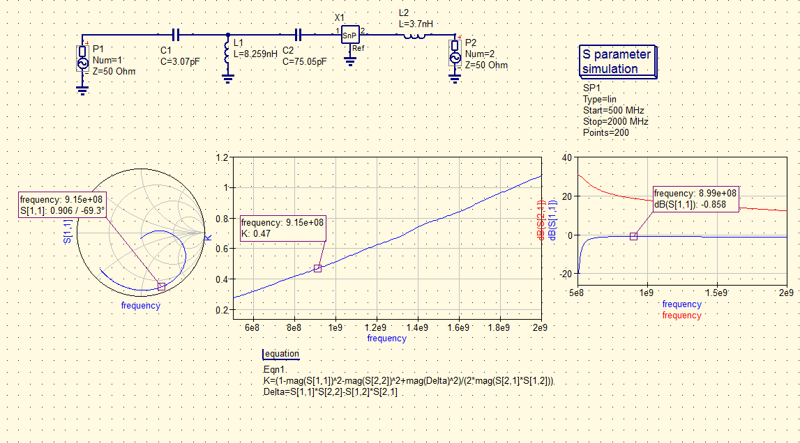
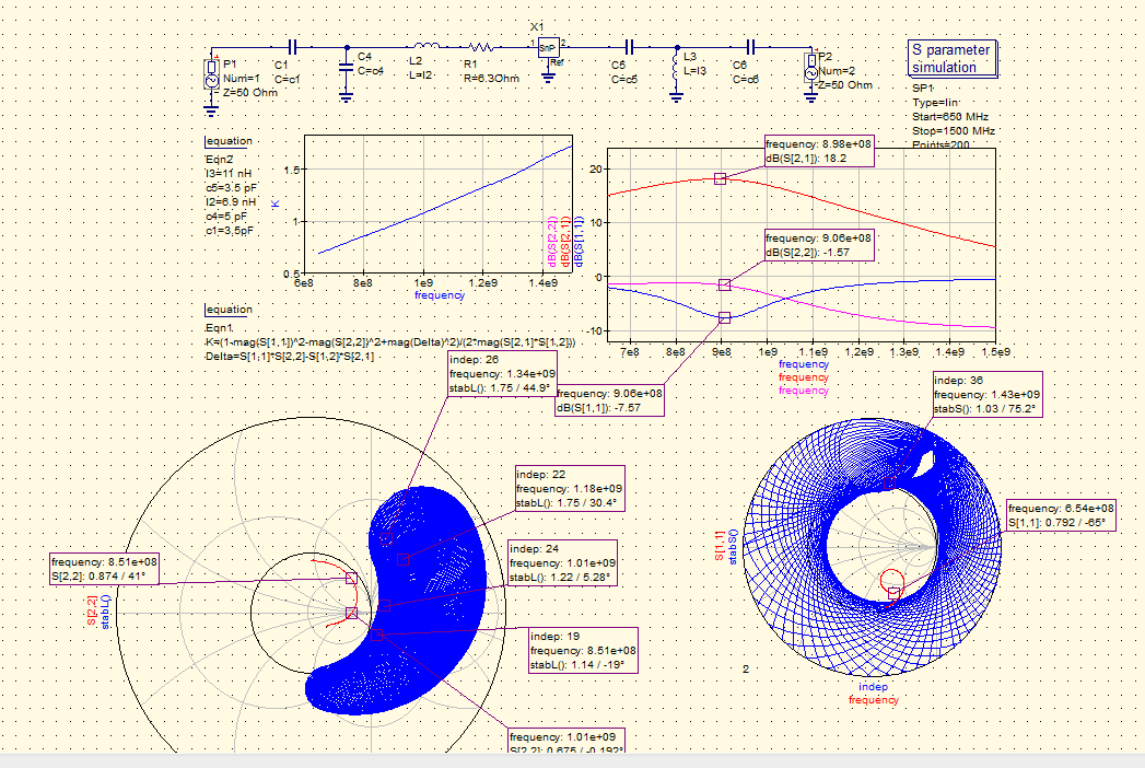
From the Sparameter model from the website i simulated the amplifier but the S parameter values are at 900 MHz is not less than -10 dB. After analyzing stability parameter K , the amplifier is not stable in that frequency.
Attachment 151518
please help me to find proper design for the power amplifier ?
It seems that you got confused with the optimal source/load impedance. The datasheet says 52.6+ j22.8 as the optimal load impedance. But you put a capacitor in series, this will end up with load impedance of 52.6- j22.8. Probably the same for the optimal source impedance.
i put it for conjugate matching.
Just have a quick look at the datasheet. My understanding is that you should have 52.6 + j22.8 as the optimal overall load impedance. This means that the output impedance of the amplifier is 52.6 - j22.8. Now the overall load impedance must be negative-imaginary part since you insert a capacitor in series.
Your Output Matching is not correct..
as per your comment i did the simulation. Still the stability parameter is not greater than one in 900 MHz. The input reflection coefficient is not less than -10 dB. Can you please tell me where i am wrong ?
The problem may come from the s-parameter of your amplifier. Have you double checked that the amplifier s-parameter matches with the datasheet? As you can see, different IQD affect the input/output impedance significantly.
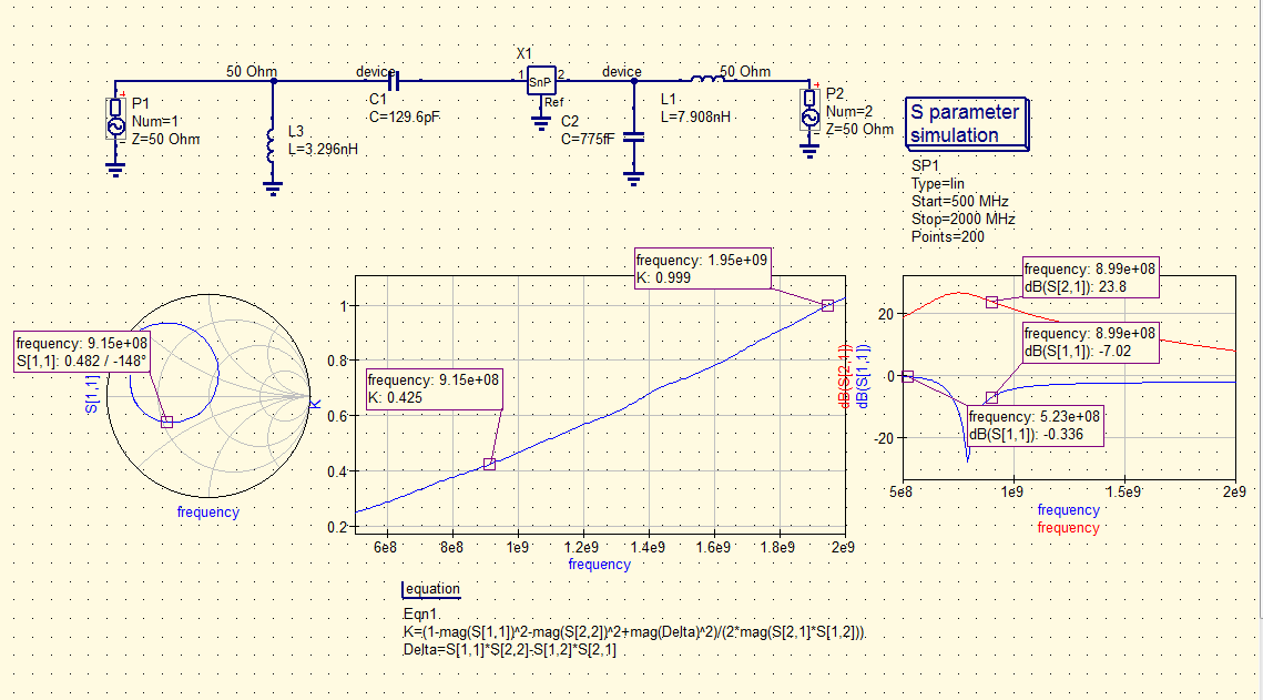
i wrongly entered the impedance value in the simulator. Now i matched both in put and output, still the amplifier is not stable in that region. Can you help me to stabilize the transistor?
Could you plot the S12 as well? The isolation is also critical for stability. I also notice that your S11 and S22 are still too high. Try to make perfect match at the central frequency. If the K is still not large enough in the band of the signal, try to use higher-order matching network to increase the matching bandwidth.
Alternative solution is to add attenuation at input/output or both. This will reduce S21 and S12, also reduce S11 and S22. The stability will be higher by sacrificing the gain and noise figure.
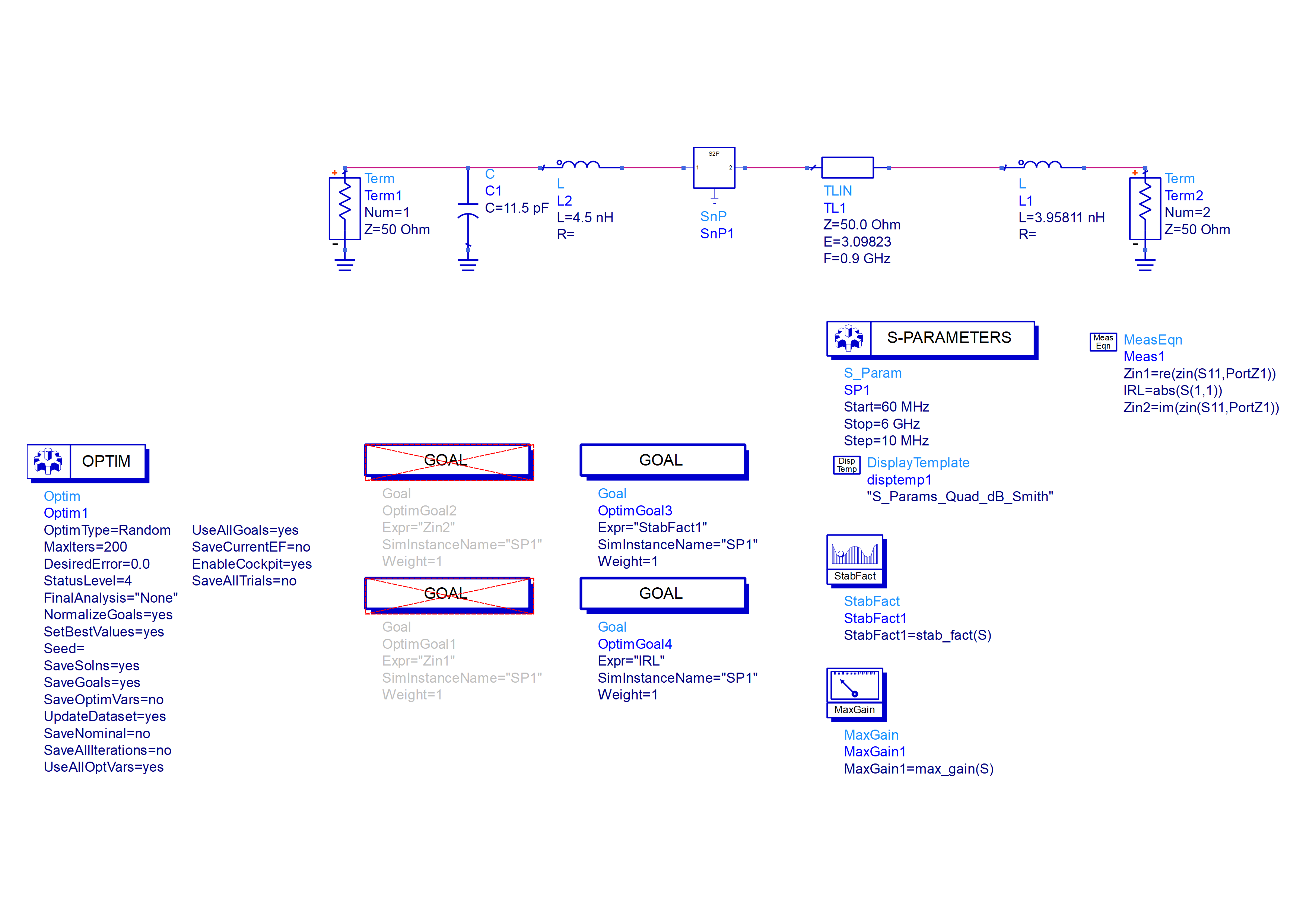
You should study more on how to design an amplifier concept.Having a Stability Factor less than Unity doesn't say that the Amplifier will absolutely oscillate.It's a Conditionally Stability state and many Power Amplifiers work at this state.You can find a solution practically by tweaking if you wish a Unconditional Stability but this might not be possible in every time.

Just remind another thing. The S-parameter is obtained by assuming ideal load/source terminations. For your case, you need to optimize both input and output impedance. When you put an impedance matching network at output, the input impedance is NOT the same as S11 of the amplifier any more since your load impedance is not 50 Ohm. That is probably why you didn't get the perfect S11 and S22.
The solution of this problem is either optimize the input and output impedance in the same time, just like BigBoss did. Another solution is to optimize the input and output impedance iteratively:
1. First put an output impedance matching network based on the the S22 of amplifier. Then you will get zero reflection at output port, in the condition of ideal source impedance present at the input port;
2. Calculate the S-parameter of the new network composed by amplifier and output impedance matching network. We have obtained that S22=0 after step 1;
3. Find the optimal input impedance matching network based on the S11 of the new network composed by amplifier and output impedance matching network;
4. After inserting the optimal input impedance matching network, you will get S11 = 0 of the new network composed by amplifier and output impedance matching network. But the S22 of new network composed by amplifier and input/output impedance matching network will not be zero any more;
5. Resign the output impedance matching network based on the S22 of the network composed by input impedance matching network and amplifier;
6. Resign the output impedance matching network
....
Until both S11 and S22 are satisfied.
Of course, if you have the tool that can optimize input/output impedance matching network in the same time, thing would be much easier.
now i matched the transistor and added one 6 Ohm resistor in series with the input. Now the transistor is conditionally stable. I matched the transistor for maximum power so is it necessary to get S22 less than -10 dB ?
Yes, since your load is 50 Ohm ideal, maximum output power = minimum returnloss.
It sees that S22 is still too high.
You still try to match S22.. Power Amplifiers don't use S22 to get max. Output Power.
Optimum Load Impedance has already been given in the datasheet, what you otherwise are looking for ?All you have to realize a Output Matching Circuit that present this Optimum Impedance to the Transistor..Input Presented Impedance is also given, design your PA under these circumstances..that's it..
BigBoss is right! I also got confused. Actually you just need to do reverse impedance matching, let the source/load be the same as the datasheet requirement. If the K is not good enough, just add a small attenuator to make sure the stability.
If i want to change the VDS value to 32 voltage and maintain the 50 mA Ids then optimum load data given the datasheet will change ?
S22 is generally not important for RFPAs. The load impedance is determined for optimal output performance, not for conjugate matching. As for S11, usually the input matching network is designed such that S11 is small. -10dB is not too bad. Often stability and S11 can be improved by adding gate shunt resistors, though this will also decrease the overall power gain.