PA loadpull impedance location
I see a lot of PA design toturial, why the optimized impedance of the load-pull simulation is always at the left upper cycle ( the dot red cycle) region? Thanks.
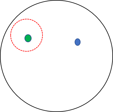
Usually the output impedance of a PA is low (or very low) depending by the output power and on how close the last stage is near compression. So the impedance point is placed on the left side of the Smith chart.
The output impedance point is placed on the upper side of the chart (inductive) or on the lower side (capacitive) depending by many factors, including transistor type (BJT, MOSFET, etc) and PA characteristic and topology (single ended, push-pull, parallel, etc).
-First, The place of 36 Ohm isn't correct, it must be on the Real Axis-Left Hand Side..( I presume the Characteristic Impedance is 50 Ohm )
-Second, Load Pull Impedance has three options.
>For Max. Gain
>For Max. Efficiency
>For Max Output Power
You have to find a compromise or an optimum point between these three points.I mean, the Impedance Matching Circuit has to satisfy one or more specifications depending on what you mostly interested in.
Third, Load Line Value is approximated one and it's been greatly linearized so Load Pull Data may quite differ than this..