what design specifications are important in pcb manufacturing for LNA's?

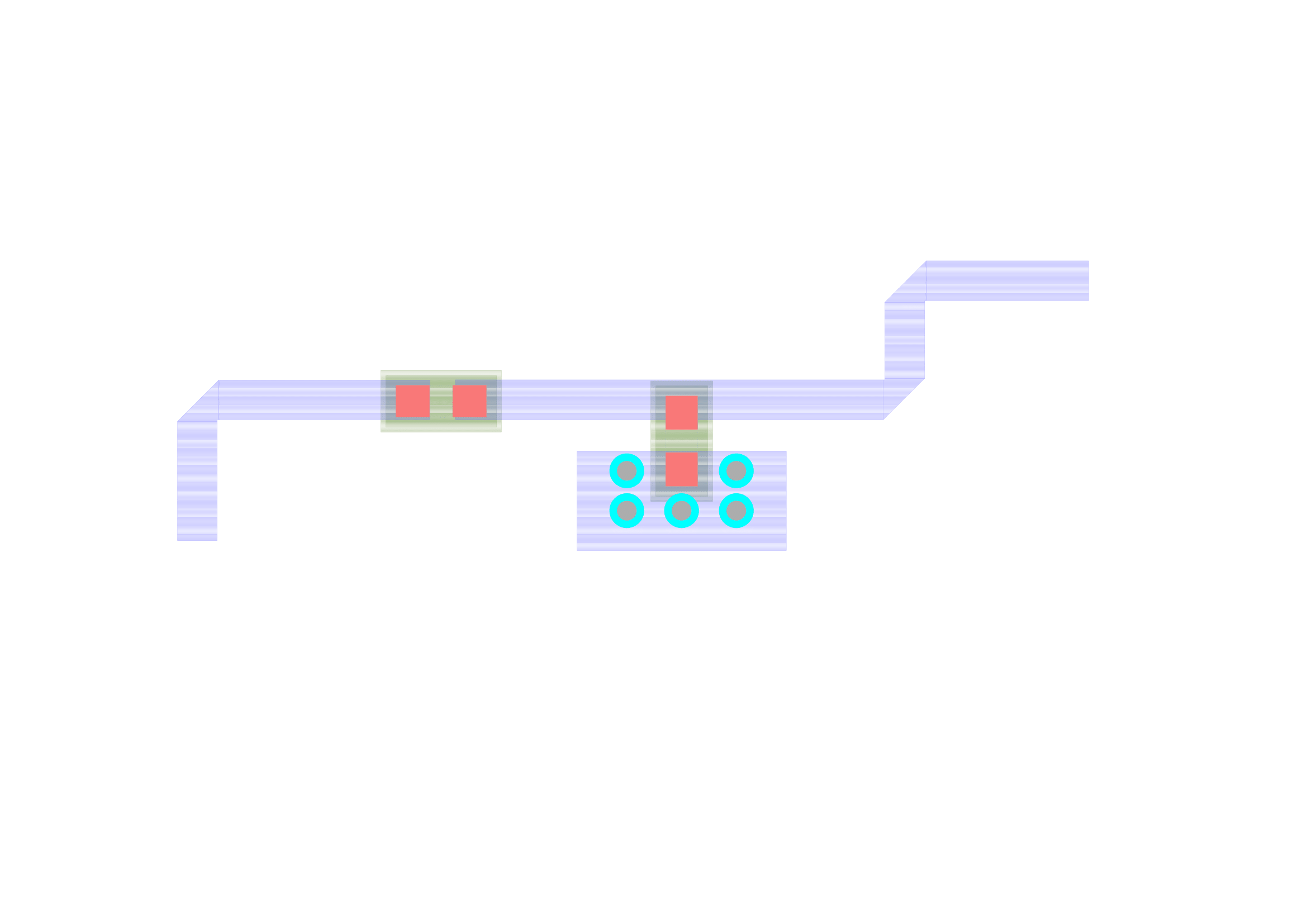
please let me know if there is anything that might concern the performance of my LNA. here is a picture of my PCB design in Eagle also:

Thanks
-GND vias are too few.Add more more vias underneath and closer to associated components.The most important thing !
Especially underneath of the transistor's emitter or amplifier's common pins whatever is otherwise you LNA will oscillate.
-Silkscreen and solder-maks is not necessary.But immersion gold plating may improve the performance.
-Bottom side will be entirely GND and there fore use a proper SMA connector with slot for PCB.Solder well both sides.
https://uk.rs-online.com/web/p/sma-connectors/5265763/
-FR-4 fine for 2.4GHz but less loss substrate is preferred.( design can be changed )
Why didn't you post your pic here? There isn't enough of a pic to make any really valuable insights. FR-4? I wouldn't use it in a manufacturing run because the dielectric constant isn't well enough controlled. Also, the loss tangent is rather high for microwave work. If it is used, there better be a lot of excess gain and noise figure in your design to overcome the deficiencies of the material.
I agree with BB that more vias are good, as is a FULL ground plane on the backside. Also, silkscreen and solder mask over your microwave traces actually degrade performance (it's like an additional piece of PCB core layed over the traces). I would have designed using Co-Planar Waveguide (CPW) to design your LNA. This allows (requires) ground to be flooded on the TOP side also.
At 2.4GHz, you can get away with these deficiencies for a lot of designs, but not all. If you're going to be the person fixing all the bad production boards, then you might want to reconsider the design philosophy.
For the paths between the SMD and paths to ground, you have used the same line width as for the 50 ohm lines. That is not required, and makes these paths larger (longer = more inductive) than necessary. I would use shorter smaller lines there, trying to make the circuit a lumped circuit without excessive interconnect length.
You are using heat relieved traces to connect your SMA connector to ground. That is a disaster - don't do it. For a μwave PCB, never use heat relief. Always use full ground flood.
Why do you still have air wires on all the connections? You must be doing something wrong in your PCB package.
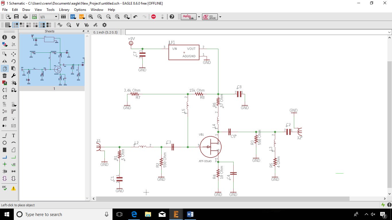
Where is your schematic? Without one, it is difficult to identify the critical circuit paths.
What are your design specs?
here is my schematic for reference:

- Why do you say add more vias? why isn't 1 via good enough to suffice a shorted stub? I used a bypass cap (100 pF) and 10 ohm resistor (for stability). I was thinking it would be nicer to have the vias connected to a very small piece of copper (enough size for the via and the conductive material on the component) so that the components can be soldered to a metal piece, rather than being accidently soldered to the FR4 board (having the via underneath the via). BTW, doesn't adding a transmission line for a common source help stabilize a microwave amplifier?
- I might try the gold plating, unless it very expensive?
- The SMA (0.042'') that I picked should be a good fit for the FR4 board (0.04''), should the bottom be fully covered with copper all the way to the edge of the board (entirely GND)?
- what would be the best substrate to use other than FR4?
when I put a via on the transmission line, I specified that the name was GND, meaning that the via is connected to GND
You forget working at 2.4GHz.Everything is critical at RF.
Typical GND connection of a stub or grounded components should be as follows.

so, a typical GND connection at 2.4 GHz has 5 vias surrounding one terminal end of an SMD component? why is this? instead, as you said before, would I be able to just have 1 via underneath the component instead of having 5 vias surrounded?
One via has approximately 1nH of inductance. 5 in parallel has 1/5 of that inductance. 10 in parallel has 1/10 the inductance. Get the picture? Carried to the extreme, an infinite number of vias would have 1/∞ inductance, or zero.
what if the whole via is covering the whole end of the component? would that be 1/∞?
Try to re-invent the square wheel?
Vias in pad have restriction. They must be either very small or "plugged" and preferably the plug copper plated to be suited for regular SMD solder process. They still expose a finite inductance. The suggested via arrays, or CPW copper pours with via fences are the best way for the ground connection of shunt elements.
It's not that simple, because RF current will prefer the lowest impedance path. Adding more vias that are too far away doesn't help at all. Many years ago, I showed this EM-based via analysis in my trainings:
Via_Inductance.pdf
Anyway, comparing that lumped element schematic with the layout, I believe that all those extra line lengths will cause a lot of trouble. The layout could (and should) be drawn a lot smaller, reducing parasitic layout effects.
FR4 substrate material isn't a big issue problem, because by design this is essentially a lumped circuit. Just take out all that unneceesary extra length and the substrate influence will be small.
- So what would you recommend as a via, instead?
Closely spaced vias, as in BB's example.
I recomment that you design using CPW as your structure. With ground on top, there is no need for stub vias.
you mean this area can be smaller in size (circled in red): https://imgur.com/a/78JiNuZ? I got the via and component as close as possible (tangent), except for the one at the far top left of the board (I was thinking I probably should shorten that one also).
I am using Eagle PCB software and I don't think there is CPW (this is the first time I've heard about CPW) feature to use, is there? I think I might just use the closely spaced vias (5 of them), but what size via would you recommend? my transmission line is 0.077'' in width and using 0402 components.
Most PCB packages don't have a CPW "feature" - in fact, most don't have any μwave features. But setting it up in Eagle is a piece of cake. Just determine what width of trace you want and the ground separation, then set the appropriate distance. I've used Eagle for this quite often. In fact, most PCB packages can be set up to do "CPW" with little effort.
It would behove you to look up what a CPW is and does and place that knowledge in your quiver of useful tools, especially for μwave design. No offense, but why were you chosen to do the design?
here is my schematic for reference: https://imgur.com/a/5l7yMnV
What do you mean by heat relief? My intention is to have full copper underneath the FR4 board; all the way to the four edges of the board (0.04''). I am also using a 0.042'' SMA and I intend to solder each arm of the SMA onto the full copper underneath. Is my PCB simulation different than what I intend for?
When I start out the design for PCB I always get air wires, do I need to delete them? do the air wires effect my PCB circuit design or something? would this effect the manufacturing process?
My design specs are: 2.4 GHz and the highest possible gain using lumped components.
I was the one who chose to do this and I am the one who is designing it.
Are you sure about that?

This image appears to show heat relief under the SMA (what is this, a camera shot of your screen?). This is a disaster. Also, your vias on the backside probably also have heat reliefs, but there isn't enough resolution to tell. IIRC, right click on the ground plane, select "Properties", then deselect "Thermals". Do NOT use Thermals on any μwave board - I go one step further and NEVER use thermals.
When you talk about CPW, is that the same thing as GCPW? I looked it up on youtube and a guy said that GCPW is better for frequencies above 30 GHz. Since I am only working at 2.4 GHz, then using microstrip, I believe would be more cost effective and less design to deal with. I think I will go with BB's example. Thanks though, I will keep that in mind next time. I want to try microstrip first, then I might consider the other.
Well then, Youtube has spoken - you can't get any more of an authoritative source than that. I mean, where else can you go to get designs on perpetual motion machines and free energy from magnets?
Anyway, your "expert" on YT is stupidly wrong. CPW (that's Co-Planar Waveguide) is better for almost all RF frequencies - plus, it is easier to implement than straight μstrip as you are finding out. I have always used the grounded version of CPW.
important specifications design 相关文章:
