Microwave amplifier, component distance
I want to know how to put the bypass and blocking capacitor and inductor in this circuit?
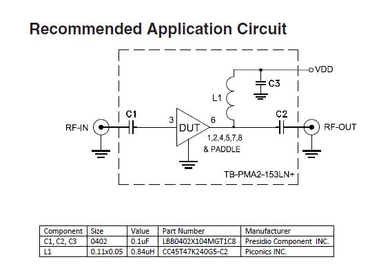
How can I define Capacitor and Inductor distance from the chip and their line track?
As far as I can tell the following links should give you all the information you need
https://www.minicircuits.com/pdfs/PMA2-153LN+.pdf
https://www.minicircuits.com/pcb/WTB...153LN+_P02.pdf
https://www.minicircuits.com/gerber/TB-PMA2-153LN+.zip
L1, as close as possbible to IC
C3 very close to the end of L1 with strong GND connection.
Thank you.
Do you have any information about the many via(s) in RF circuit design? how to calculate their hole and distance from each other?
Easiest way for you to learn is, look at an eval board of a commercial amplifier at your frequency of interest. Download it's gerber file, and look at it's via placement and size. Analog Devices and minicircuits supplement them for free. There are online gerber viewers in internet, so you don't need a program on your pc to do that.