Procedure to find optimum inter-stage matching in stack amplifier
Below is the procedure I am followed but I haven't got the required output power.
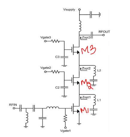
1.I found Zopt1 for M1 using Loadpull without connecting M2 and M3. Doing loadpull, I got optimum load Zopt1 as 82.015+j45.73 with output power 10.22 dBm(say) (Pin=0 dBm).
2.Next, I took only M2 (No M3 also) (Maintaining the same voltage values around it that would have if it were connected in the full circuit as in the attached figure) and to its source connected a port giving Zopt1 value in it. This time I got it's optimum load impedance Zopt2 as 71.7474+j115.152 with output power 4.05 dBm(say, pout2).
I would like to know whether
1. I am doing it in correct way,
2.Why output power(pout2) is less than pout1.
Thanks
Matching for M1 is not very correct because you neglect S12..Similarly, while you're matching for M2, you assume that S12 is zero etc..
Matching starts from the last stage with a fixed load termination then finally you match the Optimum Source Impedance to 50 Ohm..
Optimum Source Impedance for min. NF is used for M1 only, the other match impedances should have max. Gain/Flatness or optimum Intermodulation etc. because NF is mainly defined by M1.
I recommend you to use simultaneous matching technique that is available in almost every RF Design Simulator.
How to take S12 into consideration. Which parameters do I need to look for? Does it change my optimum load impedance?
I am working on power amplifer. If Matching starts from the last stage, doest my optimum load impedance change again after doing interstage matching at the output of M1 and M2(considering optimum load impedance at their drain terminals).
Since It is power amplifier, I am ignoring NF. However, to do simultaneous matching I should use noise circles and gain circles right.
You are misunderstanding.
Simultaneous matching has no relationtion to NF.
OK, it's now clear. I didn't see that it's an Power Amplifier what I thought Low Noise Amplifier..
The case is simple.. You should match the Last Stage for Optimum Load ( Source Matching can be neglected/facultative so other stages are not connected at all) ,then find Input Impedance of the last stage, then match second stage to the last one by considering either max. Power OR max. Gain or max. PAE.( Because Optimum Match can be done in these three ways) after that go like this.. The first one will be matched 50 Ohm for max. Gain because Power Efficiency or Delivered max. Power cannot be considered at that stage..( no necessity )
Oh I thought simultaneous gain and NF matching. Does it mean simultaneous input and output matching, I am not sure about this?
No.
Yes.
To find input impedance at the input of M3, I usually disconnect other parts of the circuit, keep port and maintain bias conditions and then run S parameter simulation. I would like to know if there is any other way to find this without disconnecting the rest of the network.
I hope you're saying this for the input match of M1 and I should do the output match at M1 same way as that of M2 output.