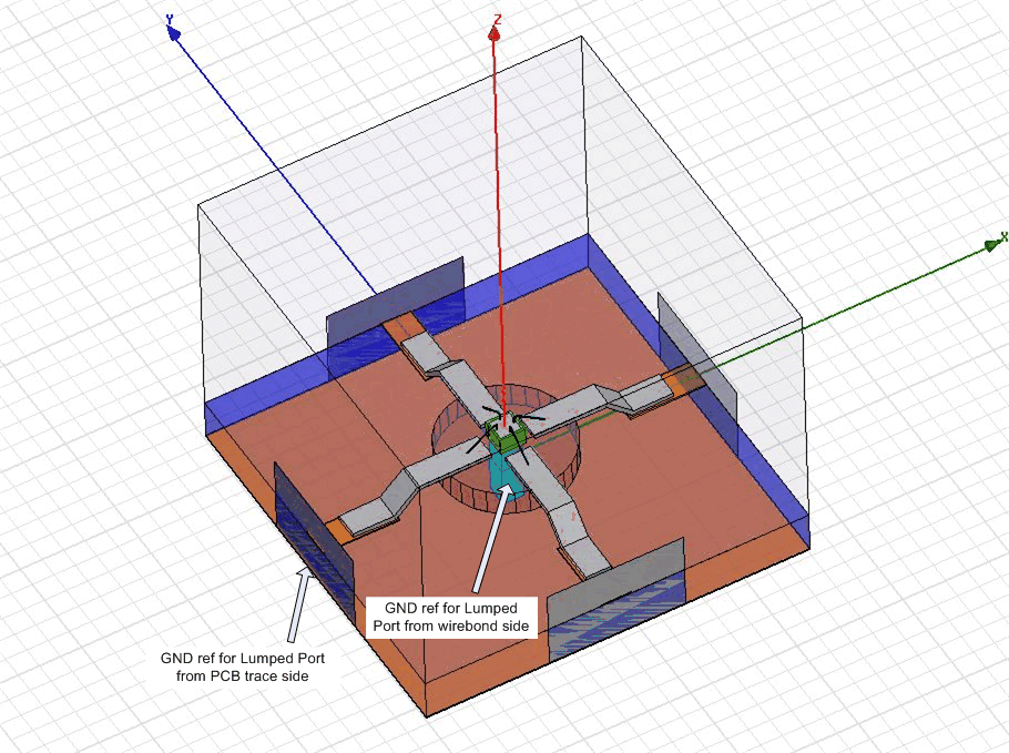
HFSS package simulation
Maybe PCB ground or exposed pad under mound.
Here the package model. I have drawn the blue box (pec material) to make ground reference for the lumped ports from wirebond sides. The HFSS simulation results in good agreement with Q3Dextractor results. But are there another way to simulate the package without the blue box?

what is the blue box? the radiation boundary?
The blue box is PEC material which serves as ground reference for lumped ports from wirebond side. I'd like extract RLC model for the package in HFSS.
are you defining the blue box as an infinite ground plane? because, if you are, can't you use a small patch, and label it infinite ground plane?
Sorry for long time without answer.
I did not define any infinite ground planes. If I do this the infinite ground plane (on chip) will cross other objects of the package 3D model...
It seems to me, that I solved the problem :) I am using export to fullwave SPICE now. In this way I can define arbitrary ground reference for ports and effectivly use it in circuit simulator. The results from circuit simulator with the fullwave SPICE model are meaninfull so I think it is ok.
