PCB and schematic simulation for CE with CST
时间:03-29
整理:3721RD
点击:
Hi guy,
i'm currently doing pcb simulation with CST. i have some basic question to ask here.
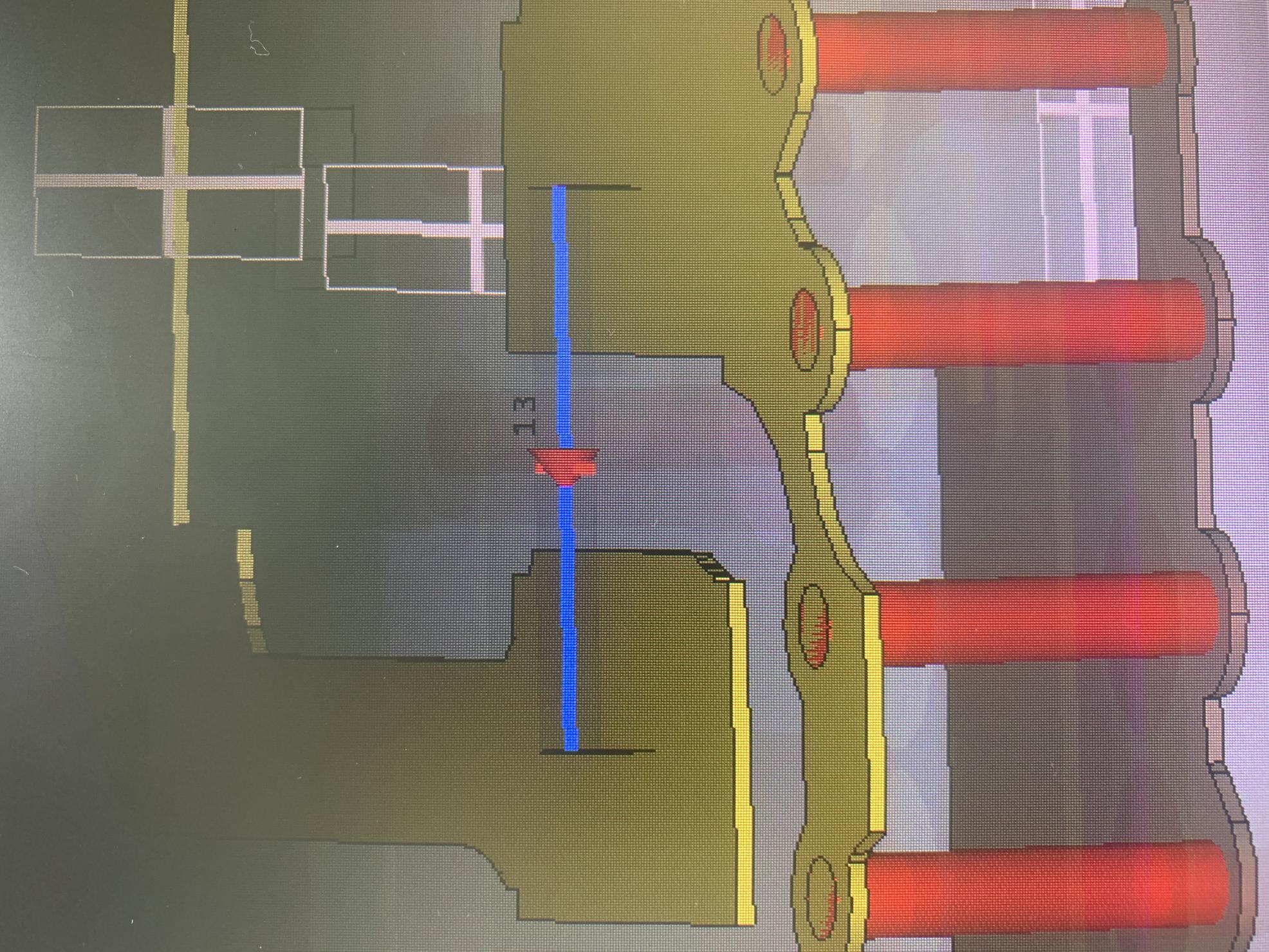
let say i assign a discrete port in my PCB for a series component as shown in figure below
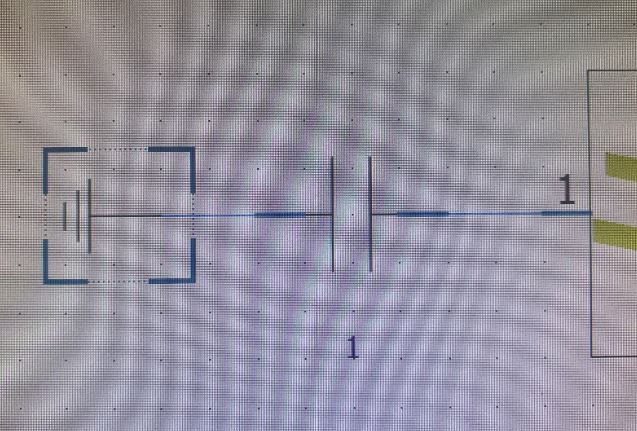
In schematic tab i assign this discrete port as lump component. the connection is shown in below. am i doing it right, by terminating the other end with a ground.
one more question if i replace it with a series resistor, i wanna probe the signal after the series resistor, which side i should place the probe in schematic tab, the ground site or the other side?
hope someone here can answer my question.
thanks
i'm currently doing pcb simulation with CST. i have some basic question to ask here.
let say i assign a discrete port in my PCB for a series component as shown in figure below
In schematic tab i assign this discrete port as lump component. the connection is shown in below. am i doing it right, by terminating the other end with a ground.
one more question if i replace it with a series resistor, i wanna probe the signal after the series resistor, which side i should place the probe in schematic tab, the ground site or the other side?
hope someone here can answer my question.
thanks
Yes, that creates a connection from the ports plus terminal to the ports local reference.
If your port represents a series element, then both is wrong. You need to probe voltage against the "global" ground where the input ports refer to. Which means you need another port that has ground reference connected to that global ground.
sorry u mean if it reprensent a series element then i cant place ground on the other side on the schematic tab?
- Assigning a circuit(Schematic) to IC in PIPRO, ADS
- How to calculate radiation from pcb edge with magnetic current ?
- Traces on PCB at 2.45 GHz
- s parameters simulation for 2 layer pcb in cst and siwave
- CST Postprocessing of multiple S-parameters (single frequency parameter extraction)
- Shielding Simulation in CST