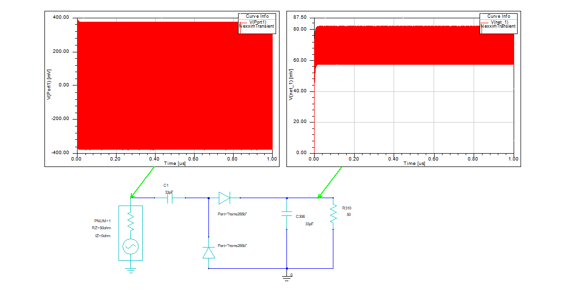
How to calculate the load impedance using ADS2015?
I know this is a very basic issue, but I'm new to ADS and I'd like to make sure my understanding is correct. Below is my schematic in ADS. I'm using S-parameter simulation. I got the values of S11, Z11, Zin in complex number format. I got confused about these terms:
1/ Zin and Z11, which is the input impedance of the circuit (hereafter mentioned as "ZLoad"), meaning the impedance looking towards the structure (including C1,C2,D1 and Term2) from Term 1?
2/ When I tried to calculate ZLoad from S11 using this equation:
Zload = Z0 * (1+S11)/(1-S11)
The result was totally different than Zin or Z11! So what kind of impedance the equation will give?
3/ I found an instruction here: https://www.edaboard.com/showthread.php?t=269785.
- For the first method, I'm wondering whether he's talking about this equation:

where Zin is my ZLoad, and ZL is the impedance of the circuit only, exclusive of Term2?
- For the second method (Smith chart) I really do not understand what he was talking about. How can I move towards load from Z11 if I do not know its value?
- At the same time, there is no transmission line in my circuit, which means transmission loss is assumed to be 0. So if I want to follow the above instruction, I have to add a pair of transmission line between Term 1 and the structure?
I hope anyone can help me to make clear these issues. Thank you so much and look forward to any response.
Zin and Z11 are not the same things.
Z-parameters are Open Circuit Parameters so when you're interested in Z11, the second ( and other possible ports) port must be open circuited.
Zin , it's real Input impedance derived from s-parameters while all ports are terminated.
Dear BigBoss,
Thank you very much for your comment. My 1st goal of measuring input impedance is to do the matching. My 2nd goal would be to vary the load with a variable input power to find the optimal load for this topology.
There is a very detailed clip (https://www.youtube.com/watch?v=ZUpuvQqK7ho) to teach how to do impedance matching in ADS. I'd like to follow this clip.
From your comment, I think the steps for me to do the matching will be as follows. Please correct me if I'm wrong:
1. Draw the schematic without Term2 (the 2nd port is open circuited). Get Z11.
2. Re-draw it without Term1. Get Z22.
3. Model the circuit by a Z2_P Eqn block. Z(1,1) = Z11, Z(2,2) = Z22. Different than the clip, a term2 will be used to terminate the output. I will not do the output matching network.
Question: Do I need to do the output matching network when my design is a voltage multiplier?
4. Start to do the input impedance matching as shown in the clip.
For my 2nd goal, after doing the matching, the Z of Term2 will be a variable within a range. A Harmonic Balance simulation will be used to determine the optimal power transferred from Term1 to Term2 corresponding to each Pin and Z of Term 2 (now it is functioned as a real load in practice).
Will this work? If you are familiar with ADS, please give me some suggestions. Thank you very much and sorry for a lot of questions.
Forget about Zxx, it's not your concern.
Your circuit will be pretty nonlinear, therefore you should work HB method but I think you have no experiences at all on HB, right ?
I have never seen a Optimum Load Condition for a such circuit, it's essentially a rectifier circuit, not voltage multiplier.
Optimum Load idea is valid if the circuit contains source(s) otherwise it's not possible to talk about a kind of optimum load concept.
No.
This is a voltage multiplier essentially.
This is a Greinacher Circuit.
https://en.wikipedia.org/wiki/Voltage_doubler
MPPT(Maximum Power Point Tracking) is very common in Rectifier and Voltage Multiplier.
Optimum Load is very important in Rectifier and Voltage Multiplier.
Is it a multiplier circuit even a node is grounded ?
It's obviously a voltage doubling rectifier ("Greinacher" circuit) but that doesn't change the problem in any way, I think.
Optimal load condition could be e.g. asked in the way, that you have a certain input level and vary the load resistance "Term2" for maximum absorbed power. Or you can turn it in an impedance matching problem if Term2 is fixed and you insert a matching network between the source port and the rectifier circuit.
As BigBoss stated, harmonic balance is the usual solution method.
Of course, yes.
I couldn't see what it multiplies..

Remove load of 50ohm or increase load value, e.g. 500kohm.
Is that a multiplication ?

Yes.
Can you understand Voltage-Doubler or Voltage-Multiplier ?
I can easily understand the difference between the words "Multiplying" and "Doubling"..
- How to correctly calculate coil's field strength?
- How to calculate radiation from pcb edge with magnetic current ?
- HFSS: Calculate Electric Field Inside the Substrate
- Calculate the raduis of circulair patch antenna
- Calculate input impedance with caviy model
- How to Calculate Transmission line feed Length,width and gap for a rectangular patch
