capacitivity coupled coil simulation in HFSS A 1MHz
I had some questions about my HFSS setup and results for a RFID near field coil. Forgive me if i can't provide all the details, many are "company confidential", but i will do my best to be general and provide what I can.
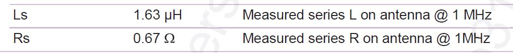
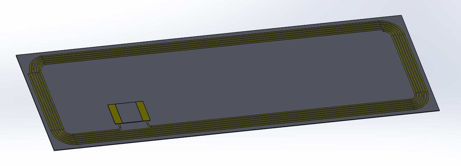
From the company that designs the RFID chip, I was given some antenna parameters to match to, see picture above. We are working with etched antenna patterns, so the two coil terminals are not physically connected, only capacitivity coupled, see picture below.
My goal is to create a simulation which can predict the series L and R for the coil at 1 MHz. I created a HFSS simulation the best I could, but have run into some questions / problems.
1) When i define a lumped port between my terminals, i am forced to choose a port impedance (which makes sense) but i feel it is perturbing my results by add a 50ohm connection which doesn't really exist. Is a lumped port really the best way to proceed here? Do you think it is wise to simply put the conjugate match [ from the picture above (Rs-Ls) ] as the port impedance?
2) From this type of simulation, what results would actually show the series Rs and Ls of the coil. Is it simply Z11? Since I am using a lumped port, Zo seems out of the question since its always 50 ohms.
I am sure there are more problems than the two I just asked, but any advice, guidance, or help would be much appreciated. I will attach my HFSS file here, its from vr 15. Let me know if you need any more details about the problem.
Thanks in advance,
Sami Hawasli
Intial testing.zip
Yes. The extra path length by the port doesn't matter at your low operating frequency. The port impedance values doesn't make any different when you calculate the resulting input impedance into the coil, to extract R and L. Just leave it to 50 Ohm.
Z11 sounds right, unless HFSS uses a non-standard way of naming output data.
Good luck!
I would be very surprised if the intended capacitively coupling works at 1 MHz.
Yeah, to be honest, I don?t really get it either. I get non sense results from HFSS. The input impedance is basically an open no matter what do I. The company that provided us the RFID chips and antenna design is 100% unwilling to help, while unsurprisingly they are still 100% willing to sell us their chips.
At this point I don?t deally know what to do other than make a coil in real life, and test it on a LRC meter to see if it is even close to the required values.
Best,
Sami
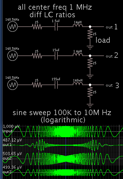
With your spec inductor value 1.6 uH, the capacitance needs to be 16 nF in order to have a center frequency at 1 MHz.
You can set series resistance to 50 ohms although that gives you a large bandpass width, according to a simulated sine sweep.
My simulation has L ratios in steps of 10x. C values are selected to obtain 1 MHz center frequency. This reveals that high series resistance gives you small bandpass effect. Series resistance ought to be low if you want a prominent rolloff curve.
Your layout shown above should give an open circuit indeed. You have two open ends, not a closed loop.
I guess, the idea behind the "capacitive coupling" is to avoid a trace crossing. But as Brad has calculated, the required capacitance values for 1 MHz can't be implemented. HFSS simulation won't help you, just confirm that the design idea is doomed to failure.
Ok, I understood that the capacitive coupling is between the pads and the RFID chip.
Obviously, capacitive coupling of these far away open ended turns will not work at all at 1 MHz. I guess there is a misunderstanding about the layout, and there is some underpass on the back side missing.
Could be another interpretation, despite of the missing loop closure in the picture. But I fear, I would work neither for 1 MHz.
In any case, the model geometry needs revision.
Since the company won’t offer any help, and I doubt anyone here is going to rip off their design:
The loops are not meant to connect. The point is to have an anteann that can be etched directly onto pcb. The drawing I showed had larger gaps than intended, in order to hide their real design. The distance between loop traces is on the order of 200um. The chip itself is a “contactless chip” which simply means it possesses a loading capacitance of 68pF. Again, the company wouldn’t spefcity, but I imagine that 68pF will be in series with loops L and R, but can’t be 100% sure on that
In any case the impedance of that 68pF at 1mhz is pretty large, and it doesn’t even match well to the proposed loop impedance. I have one of the chips, I could go stick it on the lcr meter and measure it’s input impedance just to check too.
Thanks for all your responces!
You al are the best!
Sami
From many years of experience with designing & simulating such coils: you need a closed loop to realize the inductance, your design idea with open ends will fail.
You cannot transfer layout concepts from UHF tags to low frequencies.
Sounds like a industry standard 13.56MHz chip (ISO 14443/NFC) which would well fit the 1.6 μH coil. Apparently also the operation frequency has been obfuscated?
Of course the chip is designed for closed loop coil connection.
It?s not my design idea, straight from the company (NXP) engineers. However, I agree with everything you and all the posters have posted.
This project was picked up by a bunch of 3D printer folks, who have no clue about RF anything, and I don?t really have the heart to tell the higher ups this probably won?t work. I got the tech to print an anteann, just as NXP specified, and I?m going to measure it in the morning. It will be easier to make my case with some measurement results.
Thanks again,
Sami
Your tactful outlook is probably wisest. It sounds as though 3D printing can fabricate an antenna. So it becomes easy to fabricate all kinds of experimental designs.
Your team will probably try one revision after another. You may participate in a successful project after all, if not this week then maybe another time.
Sami, assuming this is 13 MHz RFID, I'm sure there is a misunderstanding on the actual layout somewhere. Can you provide a reference to the NXP design/appnote?
Not without breaking a NDA or company confidential policy....
but i can't stop you from googling a paper written by NXP folks, "Optimizing Design of Smaller Antennas for Proximity Transponders" and looking at figure 4.
just found the paper a few minutes ago, so i might be able to answer my own question after reading it, but, maybe there is a connection between the two loop ends (the half moon and "triangle" shapes)? That would defeat the purpose of this entire project if so.
Thanks again,
Sami
Yes, absolutely.
Your experience and intuition are right on! Thanks for all the help! The lack of info from NXP was throwing me for a loop (pun intended).
One final question and I'll let this thread die: The 3D printers aren't fans of making bridging connections. Printed dielectrics and printed "wire bonds" aren't mature enough yet for any scalable process. Do you think i can modify the loop design so the only bridge connection is the chip itself?

Of course the chip can't short out the loops, but would the chip overlapping the loops change the loop's impedance enough to alter the resonant frequency? At least this way the printers can keep it all planar.
Best,
Sami
No chance to implement the design in a single conductive layer without a jumper or bridge.
Your idea makes sense to me. The chip will not alter the inductance. But I only simulated coils and never looked at the backside of the chips, if that might short circuit your turns, so I can't tell for sure.