周计划之第二周
昨天把编译环境装好了,今天开始程序的编写。
首先介绍一IAR的使用。
以前一直使用的是MDK,刚使用时有一些不习惯。
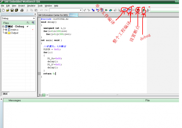
由图上可知,单个文件件的编译、整个工程编译、设置断点和debug。相信使用过MDK的童鞋都会使用。
一般入手一款的单片机,最基础的是IO的控制。所以今天做的工作就是点亮一个LED。
首先,看一看参考手册关于IO的说明
7.3 General-Purpose I/O
When used as general-purpose I/O, the pins are organized as three 8-bit ports, Port 0, Port 1, and Port 2;
denoted P0, P1, and P2. P0 and P1 are complete 8-bit-wide ports, whereas P2 has only five usable bits.
All ports are both bit- and byte-addressable through the SFR registers P0, P1, and P2. Each port pin can
individually be set to operate as a general-purpose I/O or as a peripheral I/O.
The output drive strength is 4 mA on all outputs, except for the two high-drive outputs, P1.0 and P1.1,
which each have 20-mA output drive strength.
The registers PxSEL, where x is the port number 0–2, are used to configure each pin in a port as either a
general-purpose I/O pin or as a peripheral I/O signal. By default, after a reset, all digital input/output pins
are configured as general-purpose input pins.
To change the direction of a port pin, the registers PxDIR are used to set each port pin to be either an
input or an output. Thus, by setting the appropriate bit within PxDIR to 1, the corresponding pin becomes
an output.
When reading the port registers P0, P1, and P2, the logic values on the input pins are returned regardless
of the pin configuration. This does not apply during the execution of read-modify-write instructions. The
read-modify-write instructions are: ANL, ORL, XRL, JBC, CPL, INC, DEC, DJNZ, MOV, CLR, and SETB.
Operating on a port register, the following is true: When the destination is an individual bit in port register
P0, P1, or P2, the value of the register, not the value on the pin, is read, modified, and written back to the
port register.
When used as an input, the general-purpose I/O port pins can be configured to have a pullup, pulldown or
three-state mode of operation. By default, after a reset, inputs are configured as inputs with pullup. To
deselect the pullup or pulldown function on an input, the appropriate bit within the PxINP must be set to 1.
The I/O port pins P1.0 and P1.1 do not have pullup or pulldown capability. Note that pins configured as
peripheral I/O signals do not have pullup or pulldown capability, even if the peripheral function is an input.
In power modes PM1, PM2, and PM3, the I/O pins retain the I/O mode and output value (if applicable) that
was set when PM1, PM2, or PM3 was entered.
可惜英文不好,用词典查了好久,终于有点懂了。大概就是如果要使用一个io作为GPIO,首先要设置该引脚为GPIO,然后再设置为输入或输出。
程序代码如下:
P1SEL &= BIT0;//设置为GPIO
P1DIR |= BIT0;//设置为输出
P1_0 = 0;//初始化时,LED关闭
具体源程序:
#include <ioCC2541.h>
void delay()
{
unsigned int i,j;
for(i=0;i<200;i++)
for(j=0;j<300;j++);
}
int main( void )
{
//设置P1。0为输出
P1SEL &= BIT0;//设置为GPIO
P1DIR |= BIT0;//设置为输出
P1_0= 0;//初始化时,LED关闭
for(;;)
{
P1_0&=0x00;
delay();
P1_0^=0x01;
delay();
}
return 0;
}
计划 相关文章: